
Quantifying Interfacial Solid State Diffusion Rates in Lead Free Solders
Quantifying lead-free solid-state diffusion requires Arrhenius aging matrices to enforce 4.0-micrometer IMC limits and suppress brittle failure risks.
Quantifying lead-free solid-state diffusion requires Arrhenius aging matrices to enforce 4.0-micrometer IMC limits and suppress brittle failure risks.
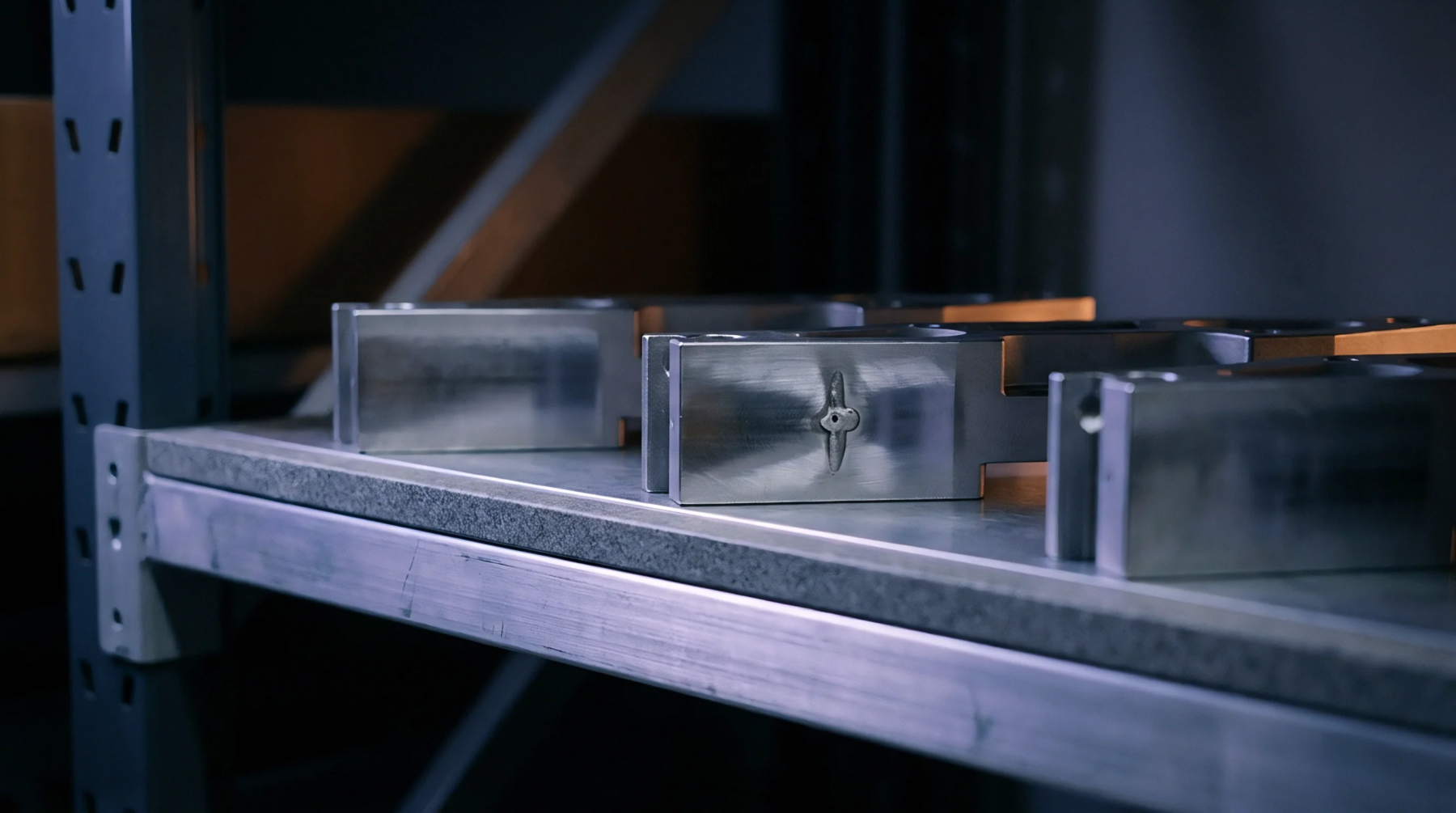
Doping tin-based solders with trace nickel, cobalt, or zinc alters interdiffusion kinetics, suppressing Kirkendall voiding and securing long-term joint strength.

Suppression of interfacial micro void coalescence requires maintaining 15-45 ppm bismuth or 200-450 ppm nickel dopants in electroplated copper to arrest vacancy migration.

Lead-free solder reliability depends on limiting Cu3Sn intermetallic growth and controlling copper bath impurities to prevent latent Kirkendall microvoiding.

Thermal gradients across microbumps drive atomic migration and voiding; mitigation demands controlling crystal grain orientation and operating flux densities.

Subcontract packaging agreements require precise metallographic defect thresholds and chemical bath audits to allocate latent Kirkendall failure costs.

Microvoid nucleation at copper surface finish interfaces stems from electroplating bath impurity co-deposition accelerating solid-state vacancy condensation.

Plated substrate interfaces demand precise nickel-phosphorus controls and tight thermal gradient limits to prevent thermomigration failure in fine-pitch packaging.

Submicron solder joint reliability requires capping electroplated copper sulfur content below 5 ppm and restricting aging Cu3Sn void area fractions under 5 percent.

Steep thermal gradients across fine-pitch microbumps drive directional vacancy migration, requiring strict interface metallurgy controls and thermal gradient modeling to prevent open failures.

Predict intermetallic growth during reflow by balancing peak temperature and time above liquidus to control Cu6Sn5 scallop thickness between 1.0 and 2.5 µm.

Unauthorized subcontracted thermal rework during post-holiday ramps creates latent field liabilities that buyers must contain through strict serial tracking, acoustic micro-imaging, and direct invoice escrow debits.

IPC-4552B compliance requires strict XRF calibration, cross-sectional corrosion rating, and phosphorus bath control to eliminate latent ENIG black pad joint failures.

High-turnover ENIG plating lines generate latent intermetallic joint failures when bath aging drives nickel corrosion past IPC-4552B Level 1 limits.

Coupled thermo-electro-mechanical fields drive interfacial vacancy accumulation, requiring precise microstructural boundary limits in supply contracts to prevent latent field failure.

Calibrate intermetallic vacancy growth by quantifying Cu3Sn void area fractions via focused ion beam milling across discrete thermal stress readouts.
Thermal aging accelerates SAC305 intermetallic growth through parabolic diffusion, where Cu3Sn layer thickening and Kirkendall voiding reduce joint shear strength.

Manage Kirkendall voiding by capping plating bath sulfur impurities under 10 ppm and clamping reflow time above liquidus strictly between 45 and 60 seconds.
Maintaining low bath organic breakdown impurities and pre-solder thermal annealing suppresses Kirkendall void nucleation in electroplated copper substrates.

Solid-state diffusion parameters dictate lead-free PCB surface finish shelf life, intermetallic growth, and solder joint reliability under thermal exposure.

Planar Kirkendall voiding and ternary phase embrittlement in electroless nickel phosphorus joints are controlled by phosphorus fraction and reflow thermal budgets.

Verify post-holiday solder joint reliability through IPC-TM-650 2.1.1 microsectioning to quantify intermetallic growth and detect latent interface voiding.

Latent packaging delamination liabilities require cross-tier contracts linking physical forensic criteria directly to multi-vendor recovery allocations.

Enforcing ENEPIG thickness windows per IPC-4556 eliminates galvanic hyper-corrosion, guaranteeing flip-chip solder joint integrity and wire bond reliability.

Sub-ten-micrometer packaging requires SPC limits set at 1.2-micrometer void diameter and 3.0 percent interfacial area, enforced by automated tool interlocks.

Mitigate voiding by controlling pad plating impurities, restricting Cu3Sn thickness below 0.8 micrometers, and optimizing underfill to eliminate triaxial tension.
Electromigration drives rapid intermetallic phase breakdown at current densities over 10^4 A/cm2, requiring barrier controls and continuous resistance testing.
Microbump mass transport flux accelerates through coupled electrothermal gradients, requiring precise flux divergence modeling to prevent interconnect open circuits.

Anisotropic vacancy diffusion along the c-axis of single-grain solder microbumps drives rapid thermomigration voiding under dynamic thermal gradients.

Microbump thermomigration drives rapid solder voiding along hot interfaces under steep thermal gradients, requiring strict thermal flux management.
Expertise is a utility, not a secret. sentiention™ publishes its working knowledge as open reference: intelligence layer covering the materials it sources, the markets it enters, and the reference that serves both.