Quantifying Latent Intermetallic Joint Failure Risks across High-Turnover ENIG Chemistry Plating Lines
High-turnover ENIG plating lines generate latent intermetallic joint failures when bath aging drives nickel corrosion past IPC-4552B Level 1 limits.

Tank
Automated electroless nickel plating lines operate continuously under heavy production loads. High-volume circuit board facilities run chemical baths across multiple operating shifts to maximize substrate throughput per hour, pumping nickel salt concentrate, hypophosphite reducers, and alkaline buffers into processing vats as square meters of copper substrate pass through the line. The chemical composition changes continuously despite automated dosing loops.
Bath aging remains the primary driver of latent interfacial defects in solder joints.
Metal turnover counts track the mass of nickel deposited relative to the initial chemical charge inside the vat, with one turnover completed when the total mass of plated nickel equals the original nickel inventory added during solution makeup. High-turnover lines running between four and six metal turnovers accumulate substantial concentrations of orthophosphate byproducts. These orthophosphate ions shift the thermodynamic reaction potential, reducing nickel deposition speed and altering the codeposited phosphorus percentage across copper pad surfaces.

Metal Turnover Dynamics and Complexing Agent Breakdown
Bath chemistry undergoes progressive physical transformations as square meters of processed copper foil strip reactants from solution. Organic complexing agents like lactic, malic, and succinic acids keep nickel ions in solution at elevated operating temperatures, but thermal stress and continuous oxidation break these organics into shorter carboxylate fragments over extended production runs. Fragmented organic acids bind nickel ions less effectively, increasing free nickel activity and disrupting controlled deposition kinetics.
Plating speed decreases steadily once orthophosphate concentrations surpass eighty grams per liter. Operators often raise bath operating temperatures from eighty-six degrees Celsius to ninety-two degrees Celsius to restore deposition speed, but that heat accelerates organic stabilizer breakdown and alters hypophosphite reduction efficiency. The higher operating temperature drives phosphorus weight fractions in the nickel deposit above ten percent, creating an excessively hard layer susceptible to internal stress accumulation.
Plating lines operating beyond maximum recommended turnover thresholds without bath replenishment exhibit accelerated nickel corrosion regardless of gold immersion duration.
The codeposited nickel-phosphorus layer forms the foundational barrier between underlying copper traces and subsequent solder connections. Standard target phosphorus content ranges between seven and nine percent by weight to ensure adequate corrosion resistance and solderability. High-turnover baths shifting toward eleven percent phosphorus yield an amorphous deposit structure with degraded wetting characteristics.
Solder reflow temperatures fail to fully dissolve high-phosphorus surface layers, leaving brittle intermetallic interfaces hidden beneath gold plating.

Autocatalytic Nickel Deposition Parameters
Maintaining chemical equilibrium within high-volume plating solution demands continuous verification of operating temperatures between eighty-five and ninety degrees Celsius. Dissolved oxygen levels, chemical stabilizer concentrations, and solution agitation speeds directly govern layer uniformity across fine-pitch surface mount pads. Insufficient fluid movement creates stagnant boundary layers inside narrow pad vias, causing localized hyper-active plating and thickness variance.
High-turnover plating lines introduce variance across large panel formats. Chemical exhaustion manifests first in high-density pad areas where localized nickel consumption outpaces automated bath dosing. Pad features on panel perimeters receive excess plating current density and chemical replenishment, while interior pads suffer from depleted reactants.
- Orthophosphate Concentration Accumulation ~ Chemical reactions continuously generate sodium orthophosphate byproducts that suppress nickel deposition speed and alter deposit morphology.
- Complexing Agent Ratio Drift ~ Breakdown of organic acids alters free nickel ion availability, driving uneven phosphorus distribution across copper trace features.
- pH Level Volatility ~ Fluctuations in bath alkalinity alter hypophosphite reduction rates, resulting in localized phosphorus weight fraction spikes above ten percent.
- Stabilizer Chemical Depletion ~ Depletion of heavy metal micro-stabilizers allows spontaneous bath decomposition, increasing background particulate contamination on surface pads.
Turnover metrics can remain within nominal guidelines even when surface discoloration stems directly from bath exhaustion rather than post-plating handling errors.
Corrosion
Immersion reaction kinetics change dramatically when hypophosphite byproducts build up inside the plating solution. Immersion gold deposition is a self-limiting galvanic displacement process where gold ions in solution exchange electrons with metallic nickel on the pad surface. Gold ions accept electrons, precipitating pure gold metal onto the pad while metallic nickel oxidizes into solution.
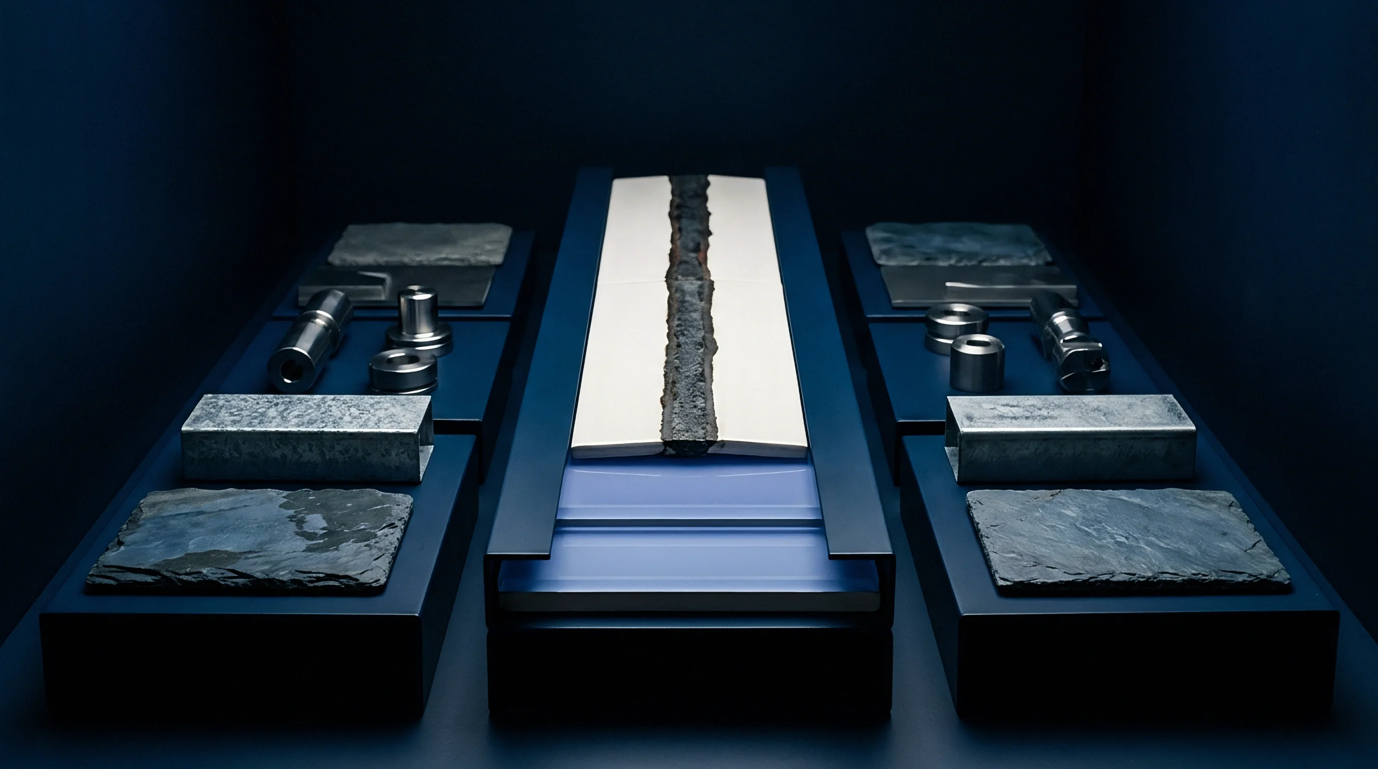
Excessive chemical activity during this exchange converts standard displacement into aggressive galvanic attack, forming microscopic fissures known as hyper-corrosion or black pad.
High phosphorus content at the surface retards initial gold nucleation. When gold plating bath chemistry contains aggressive complexing agents or operates at acidic pH levels below 4.5, gold ions attack nickel grain boundaries deeper than the outer atomic layers. Deep narrow corrosion channels penetrate hundreds of nanometers down into the nickel deposit.
Dissolved nickel leaves behind rich pockets of unreacted phosphorus that cannot bond effectively with incoming tin solder during reflow assembly operations.

Immersion Gold Strike Mechanics and Hyper-Active Substrates
Galvanic displacement occurs when copper-clad laminate panels pass from hypophosphite reduction into gold solution. Substrates with high internal stress or irregular nickel crystal orientations act as hyper-active anodes during immersion processing. The displacement reaction targets grain boundaries and structural micro-cracks, digging vertical corrosion spikes straight into the nickel deposit.
Standard quality checks fail to reveal hyper-corrosion beneath the intact gold surface layer. Immersion gold deposits measuring between 0.05 and 0.08 micrometers effectively bridge over narrow corrosion channels, concealing internal nickel structure degradation from optical inspection. The latent defect remains hidden through circuit board electrical testing, surface mount component placement, and initial reflow soldering.
Immersion gold deposits exceeding 0.12 micrometers applied over high-phosphorus nickel layers increase interfacial brittle fracture risk by 42 percent under thermal shock testing.
Excessive gold thickness exacerbates galvanic attack on the underlying nickel substrate. When immersion times extend beyond eight minutes to achieve gold thickness targets demanded by legacy drawings, prolonged acid contact deepens grain boundary corrosion channels. The plating bath continues dissolving nickel through micro-porosities in the thin gold film, creating extended sub-surface voids filled with phosphorus salts.
Phosphate Banding at the Intermetallic Boundary
Concentrated phosphorus layers aggregate directly beneath the noble metal coating during thermal processing. During solder reflow, molten tin-lead or tin-silver-copper solder dissolves the gold surface layer completely within three to five seconds. Liquid tin contacts the underlying nickel-phosphorus deposit, forming a tin-nickel intermetallic compound layer consisting primarily of Ni3Sn4.
Phosphorus is virtually insoluble in this intermetallic phase.
As tin consumes nickel to grow the intermetallic compound layer, excess phosphorus is rejected from the crystal structure and accumulates directly behind the reaction front. This rejected phosphorus forms a continuous, ultra-thin amorphous layer composed of Ni3P and elemental phosphorus directly between the nickel substrate and the Ni3Sn4 intermetallic crystal band.
The thickness and continuity of this phosphorus-rich band govern mechanical joint reliability under impact loading. Plating lines operating above five metal turnovers produce nickel deposits that form phosphorus bands thicker than fifty nanometers following standard reflow profiles. Mechanical stress concentrates along this phosphorus-rich interface during board flexing, temperature cycling, or drop impact events, precipitating sudden interfacial cleavage.
| Turnover Stage (MTO) | Orthophosphate Level (g/L) | Phosphorus Content (wt% P) | Immersion Gold Attack Severity | Latent Defect Risk |
|---|---|---|---|---|
| 0.0 to 1.5 MTO | 15 – 35 | 7.2 – 8.1% | Minimal (Level 0) | Negligible interfacial stress |
| 1.6 to 3.0 MTO | 36 – 70 | 8.2 – 8.9% | Minor (Level 1) | Low risk under standard reflow |
| 3.1 to 4.5 MTO | 71 – 105 | 9.0 – 9.8% | Moderate (Level 2) | Elevated shock sensitivity |
| 4.6 to 6.0 MTO | 106 – 140 | 9.9 – 11.2% | Severe (Level 3) | High brittle fracture rate |
Allowing hyper-corroded nickel finishes to proceed to assembly converts inexpensive bare circuit boards into unsalvageable populated assemblies destined for total scrap.

Shear
Mechanical testing reveals physical joint integrity that standard electrical continuity testing completely misses. Interfacial solder joint failure occurs along the boundary separating the intermetallic compound layer from the un-reacted nickel substrate. Standard pull testing or low-speed shear testing often yields misleading results because soft solder deforms plastically at low strain rates, masking interfacial brittleness beneath bulk solder shear values.
High-speed ball shear testing and cold ball pull testing isolate the intermetallic interface by applying rapid strain rates exceeding one thousand millimeters per second. Under high strain rates, bulk solder cannot yield plastically to absorb energy, forcing applied mechanical force directly across the thin intermetallic boundary. Fractures occurring along the phosphorus-rich layer exhibit flat, featureless brittle morphology under electron microscopy, establishing clear physical evidence of chemistry-induced joint failure.

What Triggers Brittle Intermetallic Fracture under Thermal Shock?
Coefficient of thermal expansion mismatches generate severe physical forces at the solder interface during thermal cycling. Printed circuit board FR-4 laminates expand laterally at fourteen to seventeen parts per million per degree Celsius, whereas silicon component packages expand at three to six parts per million. Temperature fluctuations between minus forty degrees Celsius and plus one hundred and twenty-five degrees Celsius generate cyclical shear forces across individual solder ball joints.
When hyper-corrosion channels or thick phosphorus-rich bands exist beneath the solder joint, cyclical thermal stress initiates micro-cracks at the root of nickel corrosion spikes. These micro-cracks propagate laterally along the Ni3P layer during repeated thermal excursions. A solder joint holding full electrical continuity during factory final test can fracture completely after two hundred environment thermal cycles in the field.
IPC-4552B Level 3 nickel corrosion findings invalidate bare board acceptance and transfer post-assembly field failure liabilities directly to the fabricator.
Reflow peak temperature and liquidus dwell time dictate the total volume of intermetallic growth. Extended liquidus times beyond ninety seconds at two hundred and forty-five degrees Celsius drive excessive tin diffusion into the nickel pad, consuming the healthy low-phosphorus top nickel layer. Extended reflow profiles thicken the intermetallic layer beyond two micrometers while simultaneously widening the brittle phosphorus enrichment zone underneath.
Shear testing isolates interfacial weak points.
Cross-Sectional Microscopic Examination Methods
Polished resin metallurgical mounts allow detailed inspection of underlying nickel crystal structures under high magnification. Quantitative evaluation requires careful sample preparation to prevent smearing soft solder across the brittle intermetallic boundary during grinding procedures.
- Extract representative pad coupons from high-density grid areas on the bare printed circuit board assembly.
- Mount the excised pad samples in clear epoxy resin and cure at room temperature for twelve hours.
- Grind and polish the mounted section using diamond slurries down to a one-tenth micrometer surface finish.
- Perform chemical etch using a nitric acid solution to expose intermetallic compound boundaries and nickel grain structures.
- Examine the polished boundary under field-emission scanning electron microscopy at ten thousand times magnification to evaluate corrosion depth.
Microscopy images reveal whether nickel degradation matches IPC-4552B acceptance standards or exhibits severe Level 3 spiking extending through more than forty percent of the nickel deposit thickness.
| IPC Corrosion Rating | Spike Depth Limit (µm) | Ni3P Band Thickness (nm) | Shear Energy (mJ) | Field Defect Rate Range |
|---|---|---|---|---|
| Level 0 (No Corrosion) | 0.0 – 0.2 | 10 – 25 | 1.8 – 2.4 | Less than 0.01% |
| Level 1 (Minor Spiking) | 0.3 – 0.6 | 26 – 55 | 1.3 – 1.7 | 0.02% – 0.08% |
| Level 2 (Moderate Spiking) | 0.7 – 1.2 | 56 – 110 | 0.7 – 1.2 | 0.15% – 0.50% |
| Level 3 (Severe Hyper-Corrosion) | Greater than 1.2 | 111 – 240 | 0.1 – 0.6 | 1.20% – 4.50% |
Incorporating IPC-4552B rating compliance directly into bare board purchasing specifications shifts total financial liability for latent solder joint separation to the plating facility.

Cadence
Establishing a strict monitoring schedule prevents silent chemistry drift before defective circuit boards enter the assembly line. High-turnover facilities processing thousands of panel square meters daily require tightly controlled chemical analysis schedules. Relying on end-of-day laboratory sampling allows hundreds of compromised panels to pass through plating lines before bath parameter shifts are identified.
Real-time analytical control protocols correlate chemical addition rates directly with total surface area plated per hour. Bath replenisher additions must occur in small, continuous increments rather than large bulk doses to maintain steady-state chemical equilibrium inside plating vats.

Plating Bath Monitoring Routines and Analytical Frequency
Laboratory technicians measure chemical constituents every four operating hours to verify solution activity. Atomic absorption spectroscopy measures dissolved nickel concentration, while automatic potentiometric titration determines hypophosphite and orthophosphate buildup levels. Bath pH requires continuous inline electrode monitoring with manual buffer calibration performed at the start of every shift.
Tracking metal turnovers requires automated panel-counting software tied to bath volume calculations. When bath aging approaches four metal turnovers, analytical frequency increases to two-hour intervals. Quantitative X-ray fluorescence measurement of plated test coupons occurs every four hours to verify gold and nickel deposit thickness distributions across panel surface grids.

Supplier Escalation Triggers for Off-Spec Bath Chemistry
Factory quality managers stop production whenever orthophosphate levels breach established control boundaries. Operating guidelines dictate clear intervention points where technical staff must pause panel processing, adjust replenishment ratios, or dump aged chemical solutions entirely.
- Orthophosphate Ceiling Threshold ~ Immediately drain and rebuild the plating bath when orthophosphate concentration exceeds one hundred and twenty grams per liter.
- Phosphorus Fraction Control Boundary ~ Reject plated lots when chemical analysis reveals deposit phosphorus weight content outside the seven to ten percent window.
- Gold Thickness Distribution Limit ~ Halt production when X-ray fluorescence measurements indicate average gold thickness exceeding one-tenth micrometer across fine-pitch pads.
- Daily Shear Force Variance Floor ~ Require line re-calibration whenever mean solder ball pull strength drops by more than fifteen percent between operating shifts.
Consider a production run processing ten thousand high-density circuit board panels through an aging plating line. Assume chemical analysis reveals orthophosphate concentration at one hundred and five grams per liter, placing the bath at 4.2 metal turnovers. XRF testing shows average gold deposit thickness at 0.11 micrometers with phosphorus weight content at 10.4 percent.
Historical yield data indicates this chemistry profile carries a 1.8 percent probability of field brittle fracture under mechanical shock. Scrapping the bare board lot at thirty dollars per unit costs three hundred thousand dollars. Allowing the lot to proceed through surface mount assembly adds two hundred and fifty dollars in component value per board, escalating potential total product loss to two million eight hundred thousand dollars if field failures occur.
Plating lines that track chemical replenishments strictly by volume rather than by throughput area inevitably produce inconsistent nickel deposits.

Settlement
Assigning financial responsibility for latent component detachment depends on clear contractual quality definitions. Standard bare board purchase agreements often cite basic continuity testing and surface gold thickness compliance as sole acceptance criteria. These basic parameters fail to protect buyers against sub-surface hyper-corrosion and brittle intermetallic structures that pass initial factory gating intact.
Contract clauses must define specific micro-sectional evaluation standards, mandating compliance with IPC-4552B corrosion level limits prior to shipment approval. Including high-speed ball shear testing metrics within purchasing specifications provides objective physical proof of joint integrity, establishing enforceable pass-fail boundaries grounded in mechanical performance.

Rework Commercial Mechanics and Scrap Cost Allocation
Component stripping and re-soldering on compromised surface finishes destroys underlying pad adhesion. Applying reflow heat multiple times to hyper-corroded nickel pads accelerates phosphorus rejection, thickening the brittle Ni3P layer underneath remaining components.
Reworking defective solder joints on hyper-corroded nickel pads accelerates intermetallic phase growth and converts latent mechanical weakness into immediate field fracture.
Commercial resolution framework agreements establish scrap liability formulas based on root cause failure analysis. When microscopic cross-sectioning confirms Level 3 hyper-corrosion as the root cause of assembly component detachment, contract terms shift total scrap value, including populated component costs and secondary assembly labor, directly back to the circuit board fabricator. Clear analytical evidence eliminates extended commercial disputes between assembly houses and raw board suppliers.
Whether real-time optical chemical sensors can fully replace manual titration without introducing uncalibrated drift into continuous plating lines remains a subject of active plant evaluation.