Meaning
Displacement reactions between metallic nickel and a gold-bearing solution create a thin protective layer that prevents oxidation and maintains the conductivity of copper pads during long-term storage and assembly. Within the scope of electronic surface finishes, immersion gold is the final metallic layer applied in the enig process to protect the underlying electroless nickel. It governs the shelf life and the solderability of the printed circuit board by providing a noble metal surface that does not tarnish or corrode under normal atmospheric conditions.
The application stops at a thickness where the displacement reaction can no longer occur, usually around 0.1 microns, making it distinct from thick electrolytic gold used for wire bonding. It is essential for boards that must undergo multiple heat cycles during the assembly of complex electronic systems.
Deposition Kinetics
The formation of the gold layer is driven by the difference in electrochemical potential between nickel and gold. When the nickel-plated board is immersed in the gold solution, the more active nickel atoms give up electrons and dissolve into the liquid, while the less active gold ions receive those electrons and deposit onto the surface. This chemical exchange is self-limiting because the gold atoms eventually cover the entire nickel surface, preventing further nickel from dissolving.
The rate of deposition is influenced by the temperature of the bath, the concentration of gold, and the acidity of the solution. If the bath is too cold or the gold concentration is too low, the resulting layer may be porous, allowing oxygen to reach the nickel and cause oxidation. A well-controlled reaction results in a dense, continuous film that is only a few atoms thick but highly effective as a barrier.
This thinness is an advantage for fine-pitch components because it does not alter the dimensions of the pads or create bridges between adjacent traces.
Surface Morphology
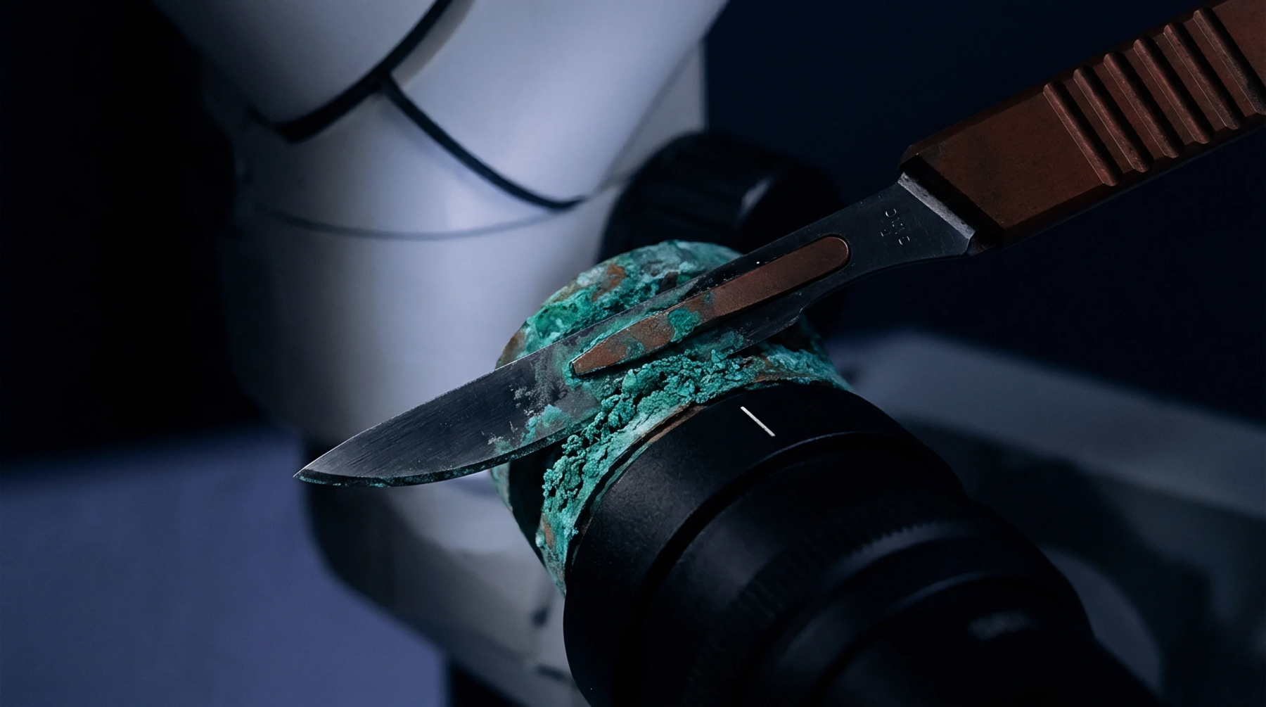
The physical structure of the deposited gold determines its performance during the subsequent soldering and testing phases. A high-quality immersion gold finish appears as a smooth, bright yellow surface that is free from pits, scratches, or dark spots. Under a microscope, the surface should show a uniform grain structure that follows the contours of the underlying nickel.
If the deposition process is too fast or the chemicals are imbalanced, the gold can form large, irregular crystals that create a rough surface. This roughness can interfere with the placement of small components or lead to poor electrical contact for testing probes. The uniformity of the layer is also critical for ensuring that the solder can wet the surface evenly during the reflow process.
Because gold is highly soluble in solder, it dissolves almost instantly, leaving a clean nickel surface for the formation of the intermetallic bond. Any contaminants trapped within the gold layer or at the nickel-gold interface can lead to weak joints or electrical failures.
Thermal Resistance
One of the primary functions of this coating is to preserve the integrity of the solder pads through multiple thermal events. In modern manufacturing, a circuit board may pass through a reflow oven several times to attach components to both sides or to perform repair work. The immersion gold layer must remain stable during these heat cycles, preventing the nickel from migrating to the surface or oxidizing.
If the gold is too thin or the nickel-phosphorus alloy is unstable, the heat can cause the formation of nickel oxides that prevent the solder from adhering properly. This results in a defect known as non-wetting, where the solder beads up instead of spreading across the pad. The ability of the gold to withstand these temperatures ensures that the board remains repairable and that the final assembly is reliable.
The selection of the specific gold chemistry and the bath parameters is based on the expected thermal profile of the assembly process. Testing for thermal resistance often involves pre-aging the boards in an oven before performing a standard solderability test.