Plated Substrate Surface Finishes for Advanced Microelectronics Packaging
Enforcing ENEPIG thickness windows per IPC-4556 eliminates galvanic hyper-corrosion, guaranteeing flip-chip solder joint integrity and wire bond reliability.


Bath
Electroless and electrolytic surface treatments define the physical interface where microelectronic substrate copper connects to integrated circuit dies, wire bonds, and board-level solder joints. In advanced microelectronics packaging, substrate copper traces require protective surface finishes to prevent oxidation during storage and to facilitate reliable assembly interconnects. Selection of the plating stack governs microbump formation, wire bond pull strength, and thermal fatigue life in high-density ball grid arrays and system-in-package modules.
Electroless Nickel Electroless Palladium Immersion Gold, designated ENEPIG, serves as the dominant multi-purpose finish for complex substrate architectures. The nickel layer functions as a structural diffusion barrier preventing copper migration into solder joints. The intermediate palladium layer prevents nickel passivation, suppresses galvanic hyper-corrosion during gold deposition, and provides a surface compatible with gold, aluminum, and copper wire bonding.
The top immersion gold deposit preserves solderability and facilitates intermetallic bonding without forming excessive gold-tin compounds.

Electroless Nickel Electroless Palladium Immersion Gold Processing
Chemical reduction reactions place metallic layers on substrate copper pads without external current. Electroless nickel plating uses sodium hypophosphite as a reducing agent, yielding a nickel-phosphorus alloy deposit containing seven to eleven weight percent phosphorus. Bath temperature, pH balance, and stabilizer concentration govern phosphorus co-deposition rates.
Controlling phosphorus content holds critical structural importance. Lower phosphorus contents yield insufficient corrosion resistance, while phosphorus levels exceeding twelve weight percent promote brittle phase formation during solder reflow.
| Surface Finish | Layer Architecture | Typical Thickness Window | Wire Bond Compatibility | Microbump Solderability |
|---|---|---|---|---|
| ENIG | Electroless Ni / Immersion Au | Ni: 3.0 ~ 6.0 µm, Au: 0.02 ~ 0.05 µm | Al Wire Only | Good (Risk of Black Pad) |
| ENEPIG | Electroless Ni / Electroless Pd / Immersion Au | Ni: 3.0 ~ 6.0 µm, Pd: 0.05 ~ 0.15 µm, Au: 0.02 ~ 0.05 µm | Au, Al, Cu, Ag Wire | Excellent |
| EPAG | Electroless Pd / Autocatalytic Au | Pd: 0.05 ~ 0.20 µm, Au: 0.02 ~ 0.08 µm | Au, Cu Wire | Excellent (Zero Ni Voiding) |
| DIG | Direct Immersion Gold over Cu | Au: 0.02 ~ 0.05 µm | Limited | Moderate (High Cu Dissolution) |
| Electrolytic Ni/Au | Electroplated Ni / Hard or Soft Au | Ni: 2.0 ~ 5.0 µm, Au: 0.30 ~ 0.80 µm | Au Wire (Soft Au) | Poor (Excess Au Embrittlement) |
Electroless palladium plating occurs autocatalytically over the activated nickel substrate using formic acid or amine-borane complexes as reducing agents. Precise bath temperature control within two degrees Celsius prevents palladium self-decomposition. Thin-film palladium deposits measuring fifty to one hundred nanometers protect the nickel surface from oxidation while maintaining low electrical resistance.
Gold deposits remain thin.
Plating panels with an electroless palladium layer between fifty and one hundred nanometers completely blocks copper diffusion during five-hundred-hour thermal aging at one hundred fifty degrees Celsius.
Immersion gold finishes utilize a displacement reaction where nickel or palladium atoms dissolve into solution to supply electrons for gold ion reduction. Autocatalytic gold baths supplement this displacement mechanism with chemical reducing agents, allowing gold thickness growth beyond fifty nanometers without attacking underlying metal layers. Direct Immersion Gold over electroless palladium eliminates nickel entirely, yielding an Electroless Palladium Autocatalytic Gold stack suited for ultra-fine pitch microbump applications below thirty micron pad pitch.

Plating Physics in Sub-Thirty Micron Substrate Features
Fluid dynamics inside narrow microvia cavities dictate local ion replenishment rates during chemical deposition. As substrate feature pitches decrease below thirty microns, mass transport limitations inside blind microvias restrict reactant diffusion. Convection currents driven by mechanical solution sparging fail to penetrate high-aspect-ratio feature crevices, causing localized depletion of nickel and palladium ions.
Fluid stagnation produces non-uniform deposit thickness distributions across the substrate panel, leading to thin plating inside via bases and thick plating on surface pads.
Ultrasonic bath agitation combined with optimized wetting surfactants lowers fluid surface tension, facilitating chemical exchange inside sub-thirty micron vias. Plating bath additives, including thiourea derivatives and sulfur-based suppressors, control deposition rates at high-current-density pad edges to prevent nodular growth. Maintaining uniform surface finish thickness across entire panel arrays prevents height variance in microbumps, which otherwise induces open-circuit defects during flip-chip die attach.
Suppliers often claim that slight palladium layer thinning below zero point zero three microns speeds up production line throughput without altering solder joint integrity.


Bond
Interfacial reactions between solder alloys and plated substrate pads determine package mechanical reliability under thermal stress. Lead-free solder interconnects, such as tin-silver-copper alloys, react with plated metallic deposits during liquid-phase reflow to form intermetallic compound layers. The thickness, crystal structure, and growth rate of these intermetallic compounds govern solder joint fracture toughness under drop shock and thermal cycling.

Intermetallic Compound Layer Evolution
Solder joint interfaces transform dynamically during thermal reflow as copper, nickel, and tin atoms migrate across contact zones. On ENEPIG finishes, molten tin reacts rapidly with the surface gold layer, dissolving it completely into the solder bulk within seconds. The underlying palladium layer dissolves next, exposing the electroless nickel surface to molten tin.
Tin and nickel combine to produce a ternary intermetallic compound composed of nickel, copper, and tin.
Nickel acts as a diffusion barrier.
When soldering with high-copper alloys like SAC305, copper atoms from the solder matrix migrate toward the interface to form a hexagonal intermetallic phase. Excess copper migration converts this layer into a complex ternary phase, changing interface stress state and grain structure. Prolonged thermal aging at temperatures above one hundred twenty degrees Celsius drives solid-state diffusion, thickening the intermetallic layer and depleting nickel from the underlying phosphorus-containing nickel deposit.

Microbump Solder Joint Phase Transformations
Lead-free solder spheres reacting with substrate metallization form distinct crystalline structures dependent on bath phosphorus concentrations. As electroless nickel reacts with tin, nickel atoms migrate into the solder joint, leaving behind an unreacted nickel-phosphorus layer enriched in phosphorus. This phosphorus-enriched band forms a metastable nickel-phosphorus phase adjacent to the intermetallic interface.
Phosphorus concentrates at the boundary.
Consider a fine-pitch flip-chip microbump with a fifty-micron solder sphere reflowed onto an ENEPIG substrate pad. During initial reflow at two hundred forty-five degrees Celsius for forty-five seconds, an intermetallic layer measuring one point two microns forms at the solder interface. After five hundred hours of thermal storage at one hundred fifty degrees Celsius, solid-state diffusion increases the intermetallic thickness to two point eight microns, while the adjacent phosphorus-enriched layer grows from two hundred nanometers to six hundred nanometers.
The accumulation of phosphorus creates localized mechanical stress concentrations, predisposing the microbump to interfacial brittle fracture under impact loads.
Gold concentrations exceeding one point five weight percent in lead-free solder interconnects induce needle-like gold-tin intermetallic precipitation that causes low-stress brittle failure under mechanical shock.

Gold and Aluminum Wire Interface Stability
Thermosonic wire attachment directly onto surface finishes requires metallic layers that resist oxidation while permitting atomic diffusion. Gold wire bonding on ENEPIG relies on solid-state intermetallic formation between the wire tip and the immersion gold coating. The intermediate palladium layer inhibits nickel diffusion to the outer gold surface during pre-heating, maintaining high bond pad surface purity.
Aluminum wire bonding forms aluminum-gold and aluminum-palladium intermetallic structures. Ultrasonic energy breaks surface oxides, allowing direct metallic contact. Copper wire bonding, implemented for cost reduction and high electrical conductivity, demands strict control over surface finish hardness and topography.
Hard nickel deposits or rough palladium surfaces cause pad cratering during copper wire wedge bonding, where energy transferred through the bonding tool fractures the dielectric substrate beneath the copper pad metallization.
Thicker gold layers improve wire bond pull strength while degrading lead-free solder joint toughness under impact loading.

Fracture
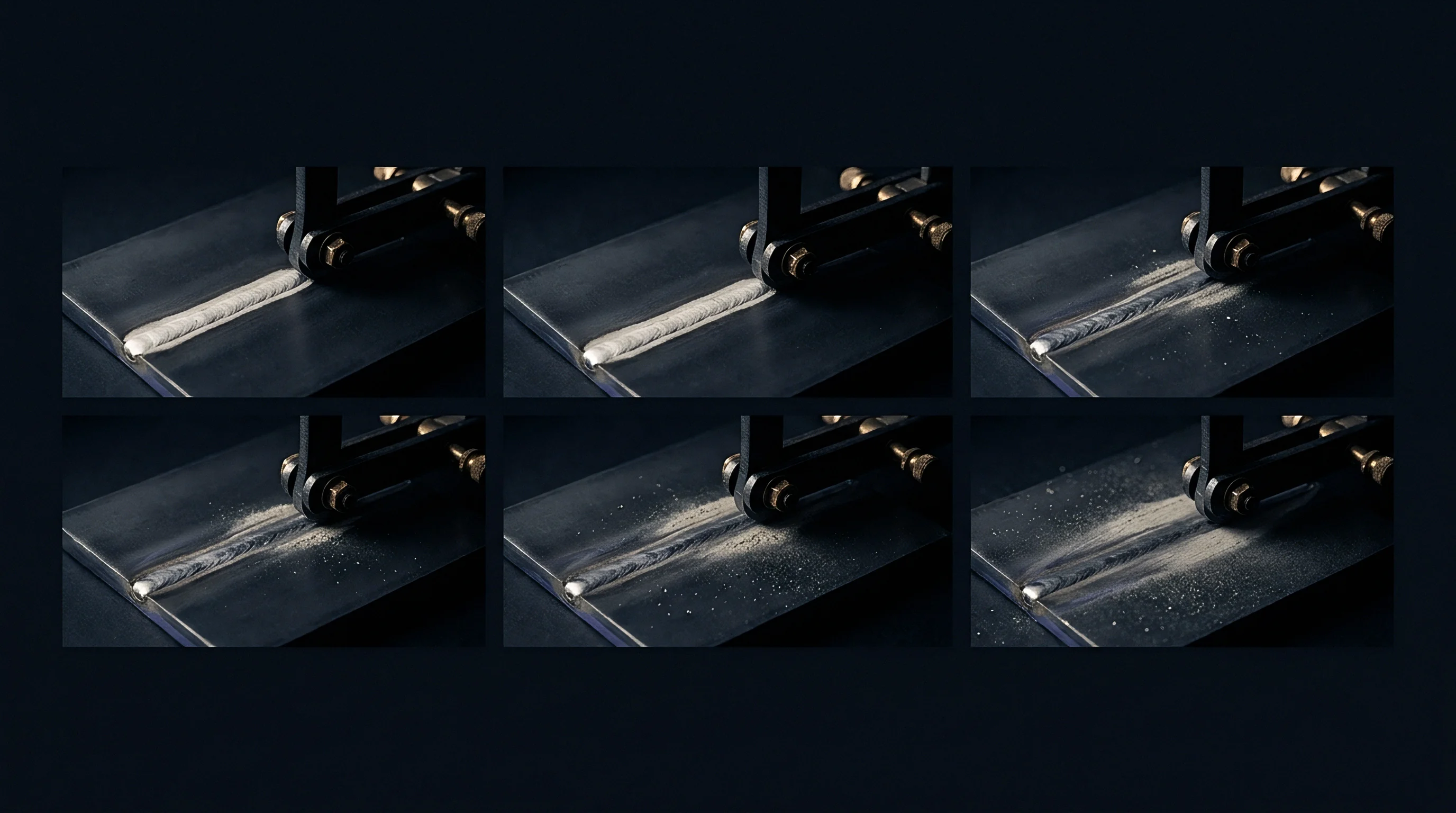
Interfacial cracking in microelectronic packages originates from chemical and structural defects introduced during board finishing. Surface finish defects remain hidden under visual inspection but initiate package structural failure during downstream thermal processing or field operation. Identifying root-cause failure mechanics allows package engineers to adjust plating parameters and bath maintenance routines before shipping defective substrate lots.

Does ENEPIG Eliminate Black Pad in Fine Pitch Packages?
The inclusion of an electroless palladium layer acts as a sacrificial barrier during immersion gold plating, suppressing galvanic attack. In standard Electroless Nickel Immersion Gold finishes, immersion gold deposition operates as a galvanic displacement reaction. Gold ions in solution accept electrons from the underlying electroless nickel substrate, dissolving nickel atoms into the bath.
If the immersion gold bath chemistry becomes overly aggressive or if the nickel deposit contains localized phosphorus variations, chemical dissolution attacks grain boundaries deep inside the nickel layer.
Galvanic attack creates deep crevices.
This localized dissolution creates deep, sharp crevices filled with dark nickel oxide and elemental phosphorus, known as black pad failure. ENEPIG prevents this galvanic attack mechanism because the autocatalytic palladium layer completely isolates the electroless nickel deposit from the immersion gold bath chemistry. Gold ions exchange electrons with palladium rather than nickel, eliminating hyper-corrosion crevices in the structural nickel foundation.

Hyper Corrosion Dynamics in Electroless Nickel Deposits
Galvanic displacement during gold immersion selectively attacks grain boundaries inside nickel-phosphorus deposits. When plating parameters drift, localized hyper-corrosion manifests as microscopic spike defects extending through the nickel deposit depth. Factors accelerating hyper-corrosion include elevated bath operating temperatures, low nickel ion concentrations, excessive immersion gold bath dwell times, and improper bath pH stabilization.
- Hyper-corrosion spikes open deep narrow voids along nickel grain boundaries that severely weaken physical interconnect strength.
- Phosphorus enrichment band forms an extremely brittle layer adjacent to the intermetallic joint interface following thermal reflow.
- Gold embrittlement voiding occurs when dissolved gold precipitates along intermetallic boundaries as continuous, brittle phase arrays.
- Substrate pad cratering manifests as micro-fractures extending into underlying laminate glass fibers caused by excessive wire bonding impact force.
- Interfacial Kirkendall voids coalesce along copper-tin or nickel-tin phase boundaries under long-term high-temperature operating conditions.

Kirkendall Voiding and Interfacial Brittle Failure
Sub-micron cavities aggregate along the boundary between intermetallic growth fronts and underlying substrate nickel. Kirkendall void formation stems from unequal vacancy fluxes during solid-state interdiffusion. Copper and nickel atoms diffuse into the tin solder matrix faster than tin diffuses into the substrate base metal.
This asymmetric mass transport leaves behind uncompensated atomic vacancies, which coalesce into Kirkendall micro-voids under thermal aging.
Thickness control prevents brittle joints.
Alternative surface finishes, including immersion silver and immersion tin, present different structural degradation mechanisms. Immersion silver deposits undergo sulfur oxidation when exposed to atmospheric contaminants, producing silver sulfide whiskers that cause electrical short circuits across fine-pitch traces. Immersion tin coatings develop compressive stresses over time, driving metallic tin whisker growth that bridges sub-twenty micron gaps between substrate pads.
Accepting surface finish lots with unmonitored bath agitation creates latent package cracking that surfaces only during final assembly temperature cycling.


Bench
Quality verification routines rely on physical, chemical, and microstructural measurement tools deployed at defined sampling frequencies. Confirming compliance with international surface finish specifications protects package assemblers against batch-level structural failures. Testing protocols combine non-destructive metrology with destructive cross-sectional micro-analysis to evaluate deposit integrity.

Non-Destructive X-Ray Fluorescence Thickness Verification
Metrology systems emit primary radiation to excite secondary fluorescence rays within metallic surface stacks. X-ray fluorescence analysis, designated XRF, measures distinct energy emission peaks to determine individual layer thicknesses across complex ENEPIG deposits. Standard single-collimator XRF systems struggle to resolve thin gold and palladium coatings on fine-pitch features due to beam spot size overlap onto solder mask material.
Advanced energy-dispersive XRF systems equipped with polycapillary optics focus X-ray beams down to spot sizes below twenty microns. Polycapillary focusing enables precise thickness measurements on microbump pads without signal distortion from adjacent dielectric features. XRF metrology requires daily calibration against multi-layer thin-film reference standards certified by international standards organizations.
XRF metrology requires daily calibration.
Industry specifications fix exact thickness acceptance criteria across plated surface finishes. The IPC-4552B standard establishes acceptable electroless nickel immersion gold plating parameters, while IPC-4556 governs ENEPIG surface finish parameters. The minimum palladium layer thickness resting on industry consensus stands at zero point zero five microns per IPC-4556, established during 2017 thermal aging trials on zero point four millimeter pitch ball grid array pads.
A buyer evaluating experimental sub-thirty nanometer palladium deposits faces unquantified risk regarding long-term Kirkendall void accumulation in microbumps under thermal shock. Under this specific uncertainty, qualified packaging buyers mandate five-hundred-cycle thermal shock qualification testing on prototype lots prior to approving bath thickness reduction requests.

IPC Standard Testing Routines and Metallographic Cross-Sectioning
Destructive cross-sectioning isolates microscopic defects across the substrate plating stack. Substrate samples are embedded in cold-curing epoxy resin, ground with silicon carbide papers, and polished using diamond suspensions down to zero point one micron grit. Etching polished section surfaces with ammonium hydroxide solution reveals intermetallic growth structures and hyper-corrosion crevices under scanning electron microscopy.
- Calibrate the X-ray fluorescence detector against certified multi-layer thin-film standards for palladium and gold thickness verification.
- Sample ten substrate pads per panel across four quadrant corners and the center region to establish coating uniformity.
- Mount selected coupon cutouts in cold-curing epoxy resin for cross-sectional grinding and mechanical polishing down to one-quarter micron diamond slurry.
- Perform scanning electron microscopy imaging at five thousand times magnification to inspect the nickel-phosphorus interface for hyper-corrosion crevices.
- Conduct high-speed ball shear testing at one meter per second velocity to quantify brittle interfacial fracture modes.
| Property Target | Standard Reference | Test Methodology | Acceptance Criteria |
|---|---|---|---|
| ENEPIG Layer Thickness | IPC-4556 | Polycapillary XRF | Ni: 3.0 ~ 6.0 µm, Pd: 0.05 ~ 0.15 µm, Au: 0.02 ~ 0.05 µm |
| Hyper-Corrosion Depth | IPC-4552B | SEM / Cross-Section | Crevices < 10% of Ni depth, Level 0 ~ 1 only |
| Solder Ball Shear Strength | JESD22-B117 / IPC-TM-650 | High-Speed Ball Shear | Ductile failure mode > 95%, Shear force > 1.5 N/bump |
| Wire Bond Pull Force | MIL-STD-883 Method 2011 | Hook Pull Tester | Au wire pull force > 0.03 N (25 µm wire diameter) |
| Plating Adhesion | IPC-TM-650 2.4.1 | Tape Pull Test | Zero metal flaking or dielectric separation |

Solder Ball Shear and Wire Pull Diagnostic Protocols
Mechanical stress testing quantifies the physical strength of substrate joint interfaces before module encapsulation. Solder ball shear testing drives a hardened chisel tool against reflowed solder spheres at defined contact heights and velocities. Low-speed shear testing at zero point one millimeter per second evaluates ductile solder deformation, whereas high-speed shear testing at one to two meters per second induces brittle interface fractures that expose plating defects.
Section 3.4.1 of the IPC-4552B surface finish specification states that nickel deposits containing Level 3 hyper-corrosion crevices over more than fifteen percent of the pad length demand immediate batch rejection.
Wire pull testing applies upward mechanical tension to wire loops using a calibrated micro-hook. Failure location tracking provides vital quality feedback. Failures occurring at the wire mid-span indicate satisfactory surface finish plating, whereas wire detachment cleanly from the substrate pad reveals poor surface cleanliness, bath contamination, or insufficient intermetallic formation during bonding.
IPC-4552B Section 3.4.1 mandates that any nickel deposit exhibiting Level 3 hyper-corrosion crevices exceeding fifteen percent of the interface length constitutes immediate lot rejection.


Scrap
Precious metal consumption and bath chemistry degradation generate measurable financial losses during substrate production. Plating process variations that deposit gold or palladium above maximum thickness limits consume expensive chemical raw materials without adding functional benefit. Conversely, under-plating causes panel rejection at receiving inspection, creating substrate yield loss that impacts package landed cost.

Gold Over-Deposition Financial Exposure
Process variability in immersion and autocatalytic plating cells pushes deposit thickness above baseline target values. Chemical bath drag-out and excess gold deposition across high-volume packaging substrate lines significantly increase raw material overhead. Controlling plating thickness distributions within tight process capability windows holds direct commercial impact.
Yield loss impacts total landed cost.
Consider an advanced substrate packaging facility producing fifty thousand panels per month. Panel dimensions measure five hundred ten millimeters by five hundred fifteen millimeters, with an active copper substrate surface coverage of thirty-five percent. The target gold deposition thickness stands at zero point zero three microns.
Process control drift elevates average gold thickness to zero point zero five five microns across production runs. Gold density equals nineteen point three grams per cubic centimeter, and gold metal spot price sits at sixty-five US dollars per gram.
Excess gold thickness equals zero point zero two five microns. The target active plated surface area per panel calculates to zero point zero nine two eight square meters. The volume of excess gold deposited per panel equals two point three two cubic centimeters.
Multiplying by gold density yields four point four seven grams of excess gold metal consumed per panel. Across a monthly run of fifty thousand panels, excess gold consumption totals two hundred twenty-three point five kilograms, resulting in an unbudgeted material expense exceeding fourteen point five million US dollars.
| Monthly Panel Volume | Gold Target Thickness | Actual Plated Thickness | Excess Gold Deposited | Monthly Material Variance |
|---|---|---|---|---|
| 10,000 Panels | 0.030 µm | 0.040 µm | 0.893 kg | $58,045 USD |
| 10,000 Panels | 0.030 µm | 0.055 µm | 2.232 kg | $145,080 USD |
| 50,000 Panels | 0.030 µm | 0.040 µm | 4.465 kg | $290,225 USD |
| 50,000 Panels | 0.030 µm | 0.055 µm | 11.162 kg | $725,530 USD |
| Calculations assume 35% substrate surface copper coverage on 510mm x 515mm panels and $65/g gold commodity price. | ||||

Chemical Drag-Out and Replenishment Unit Economics
Fluid retention on circuit panels removed from plating tanks depletes active chemical solutions. Drag-out loss carries palladium and gold ions out of processing cells into rinse tanks, requiring chemical replenishment to sustain solution concentration. Unmonitored panel withdrawal speeds increase drag-out volumes from eight milliliters per panel to fourteen milliliters per panel, accelerating chemical consumption.
Chemical drag-out increases precious metal loss.
Recouping precious metals from rinse water requires ion-exchange recovery systems. Operating recovery equipment introduces electrical and maintenance expenditures that must be factored into substrate fabrication unit costs. Efficient air-knife wiping systems installed above plating cells knock fluid droplets back into processing tanks, reducing drag-out chemical losses by forty percent.

Substrate Yield Calculations across Fine Pitch Arrays
Defect distribution models across large-format panels establish net usable die costs for advanced packaging modules. Plating defects, such as nickel skip, palladium nodulation, or surface oxidation, cause localized open circuits during assembly. In high-density substrates housing dozens of die sites per panel array, a single un-plateable pad renders the entire multi-layer substrate site unusable.
- Chemical bath replenishment records verify real-time concentration tracking for palladium salts and reducing agents.
- Coating thickness distribution logs track XRF measurements across panel quadrants to confirm plating cell uniformity.
- Cross-section shear test dossiers document intermetallic failure modes under high-velocity mechanical testing.
- Precious metal weight reconciliation statements balance input gold salts against total plated panel metal volume.
Unmonitored baths degrade panel yields.
Maintaining automated chemical replenishment systems reduces precious metal thickness standard deviation across high-density substrate panels by over thirty percent.
Whether autocatalytic gold chemistries can achieve sub-twenty nanometer deposition uniformity without increasing bath decomposition rates remains open across high-volume sub-micron packaging lines.

Contract
Commercial agreements between package designers and offshore substrate factories turn physical plating tolerances into financial remedies. Sourcing packaging substrates from overseas manufacturing hubs introduces distance risks that clear contractual language mitigates. Procurement documentation must integrate technical surface finish specifications into binding quality agreements backed by explicit commercial rejection thresholds.
Plating Specification Schedules in Sourcing Agreements
Legal supply documents reference published manufacturing standards while fixing exact chemical thickness windows. Technical schedules appended to purchase agreements must explicitly define minimum and maximum thickness boundaries for every plated deposit layer. Vague contract references to standard industry practices allow suppliers to deliver marginal thickness distributions that pass nominal receiving checks but fail during assembly reflow.
Offshore audits confirm bath maintenance logs.
Contract schedules mandate incoming chemical certificate of analysis delivery with every substrate lot shipped. Substrate shipments arriving without corresponding plating thickness distribution records or bath maintenance logs face immediate receiving holds at cargo docks. Purchase agreements should establish that non-compliant chemical documentation forfeits supplier payment terms until third-party laboratory verification concludes.

In-Line Quality Audits for Offshore Packaging Substrate Mills
On-site review of factory floor bath records confirms adherence to chemical maintenance limits. Overseas substrate manufacturers in major industrial districts often optimize line throughput by extending bath service lifetimes past chemical supplier recommendations. Operating aged plating baths generates organic contaminant buildup, leading to surface nodulation and plating porosity.
Sampling frequency scales with lot size.
Unannounced factory audits conducted by qualified technical personnel verify real-time plating line conditions. Auditors review automatic chemical dosing logs, atomic absorption spectroscopy maintenance records, and deionized water rinse purity readings. Direct floor inspection confirms whether workers maintain proper rack loading densities and sparging pressure, preventing localized flow stagnation across high-density substrate panels.

Defect Allocation and Commercial Claims Frameworks
Structured compensation rules assign cost liabilities when field failures link back to plating bath contamination. Standard substrate purchase terms often limit supplier liability to replacing raw circuit boards. This simple replacement remedy fails to protect package integrators when defective surface finishes cause assembled, fully packaged multi-die modules to be scrapped downstream.
Comprehensive quality contracts include structured scrap liability escalation clauses. When receiving inspection or assembly qualification detects surface finish defects exceeding agreed acceptance quality limits, supplier liability expands to cover wasted die costs, assembly labor, and expedited air freight charges. Implementing clear defect attribution protocols based on IPC cross-sectioning methods provides unbiased evidence for resolving commercial claims across international jurisdictions.