Substrate Dissolution and Intermetallic Compound Formation in Lead Free Soldering
Substrate dissolution accelerates in lead-free solder, demanding tight thermal controls, barrier finishes, and routine bath dilution to avoid joint failure.

Bath
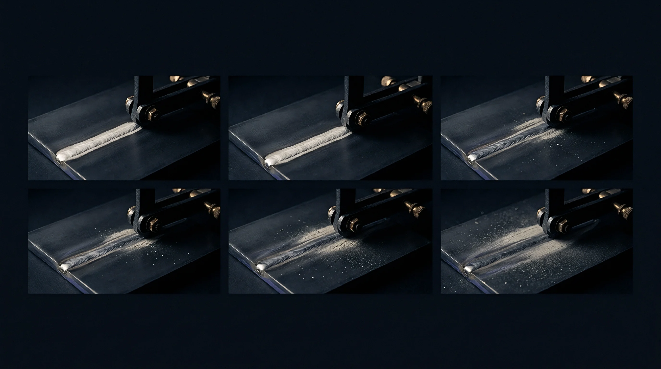
Copper dissolution into molten lead-free solder proceeds at roughly three times the rate observed in legacy tin-lead alloys. A wave solder pot or selective soldering reservoir charged with standard SAC305 (96.5Sn-3.0Ag-0.5Cu) operating at 260 degrees Celsius leaches copper traces directly from printed circuit board barrels, knee regions, and surface mount pads. Solder contact time of three to four seconds strips up to 1.5 micrometers of bare copper plating into the liquid volume.
The process operates under liquid-solid mass transfer kinetics governed by the Nernst-Brunner relation, where the dissolution rate scales with the difference between copper saturation concentration and instantaneous copper concentration in the dynamic melt.
The operational threshold sits at 0.85 weight percent copper. Virgin SAC305 enters the pot at 0.5 weight percent copper. A copper concentration climb toward 1.0 weight percent elevates the alloy liquidus from 217 degrees Celsius toward 230 degrees Celsius, narrowing the processing window and generating massive, primary copper-tin intermetallic crystals during cooldown.
These coarse Cu6Sn5 needles choke wave nozzles, bridge fine-pitch leads, and draw copper out of surface finishes before solidifying into brittle inclusions. Managing the bath demands continuous tracking of daily board throughput, surface copper exposure area, and pot turnover rates.
Controlling copper dissolution during wave soldering depends on setting pump flow velocities below 0.2 meters per second while holding pot immersion times strictly under 3.5 seconds.
Selective soldering nozzles aggravate dissolution kinetics through sustained localized liquid shear. A focused solder fountain maintains continuous turbulent flow against thin copper knee plating on thick high-layer-count backplanes. The wash effect strips the underlying copper before barrel fill achieves the 75 percent vertical rise required by IPC A 610 Class 3 standards.
Pad wash-off, barrel thinning below the 18-micrometer IPC minimum, and localized necking along the hole barrel wall develop when nozzle dwell exceeds 2.5 seconds on unpopulated or exposed pads. Production lines run into scrap rates exceeding four percent when process engineers compensate for poor hole penetration by raising solder fountain temperatures rather than addressing flux activation or board preheat deficits.

Nozzle Flow Dynamics and Copper Stripping
Liquid solder velocity accelerates the boundary layer exchange between solid copper and bulk molten tin. Laminar wave contact permits the buildup of a copper-rich boundary film that slightly retards continued dissolution. High-velocity selective soldering jets strip this stagnant layer continuously, maintaining the highest possible concentration gradient across the liquid-solid interface.
The dissolution rate jumps by a factor of 2.5 when pump speed increases nozzle fountain velocity from 0.1 meters per second to 0.35 meters per second at constant temperature.
Impingement angles generate asymmetric copper loss across component barrels. The upstream side of a plated through-hole facing the incident wave plume exhibits up to forty percent more copper erosion than the shielded downstream side. If an inner layer pad connects to the barrel on the upstream edge, thermal sinking draws additional heat while the turbulent solder flow scours the copper land.
Complete barrel breaches occur at the central knee where electroplated copper deposition is thinnest, typically measuring between 12 and 15 micrometers on lower-tier printed circuit boards.
Process audits verify copper content in wave pots using scheduled analytical chemistry. Optical emission spectroscopy or inductively coupled plasma mass spectrometry tracks copper accumulation across production shifts. A standard operational protocol dumps a portion of the bath, replenishing with a low-copper or copper-free alloy such as Sn-0.7Ag or pure tin when the copper fraction approaches 0.85 weight percent.
Neglecting the replenishment cycle leads to sluggish wave dynamics, increased icicle formation, bridging defects, and extensive board rejections during automated optical inspection.


Growth
Intermetallic compound growth at the solder-substrate interface begins instantaneously upon wetting. Molten tin contacts solid copper, initiating reaction-diffusion that forms a scallop-type Cu6Sn5 intermetallic layer directly against the base metal. During reflow profile durations of 45 to 90 seconds above liquidus, this scalloped structure thickens through rapid diffusion of copper atoms along the liquid channels separating adjacent scallops.
Peak reflow temperatures between 240 and 250 degrees Celsius yield an initial Cu6Sn5 intermetallic thickness ranging from 0.8 to 1.8 micrometers.
Solid-state aging alters the interfacial architecture. Post-reflow cooling and subsequent thermal exposure drive solid-state diffusion, creating a secondary planar intermetallic layer of Cu3Sn between the Cu6Sn5 layer and the copper substrate. The Cu3Sn phase grows at the expense of Cu6Sn5 and the remaining copper metal.
The two intermetallic species exhibit vastly distinct crystallographic, mechanical, and thermodynamic properties, altering interfacial shear performance under dynamic stress.
| Compound Phase | Crystal Structure | Elastic Modulus (GPa) | Vickers Hardness (HV) | Fracture Toughness (MPa m^0.5) |
|---|---|---|---|---|
| Cu6Sn5 (Eta) | Hexagonal / Monoclinic | 112.5 | 378 | 2.8 |
| Cu3Sn (Epsilon) | Orthorhombic | 132.8 | 343 | 1.7 |
| Ni3Sn4 | Monoclinic | 133.3 | 365 | 1.2 |
| (Cu,Ni)6Sn5 | Hexagonal | 124.0 | 410 | 2.9 |
The total intermetallic compound layer thickens parabolically with time during thermal aging according to a standard diffusion-controlled rate law, where thickness equals the initial thickness plus the square root of the diffusion coefficient multiplied by time. In field environments operating between 85 and 125 degrees Celsius, such as under-hood automotive controllers or industrial power supplies, total compound thickness expands beyond 4.0 micrometers within 1,000 thermal cycles. Excessive intermetallic thickness creates a sharp mechanical property mismatch with bulk solder, degrading high-strain-rate reliability.
Kirkendall Voiding and Interfacial Weakening
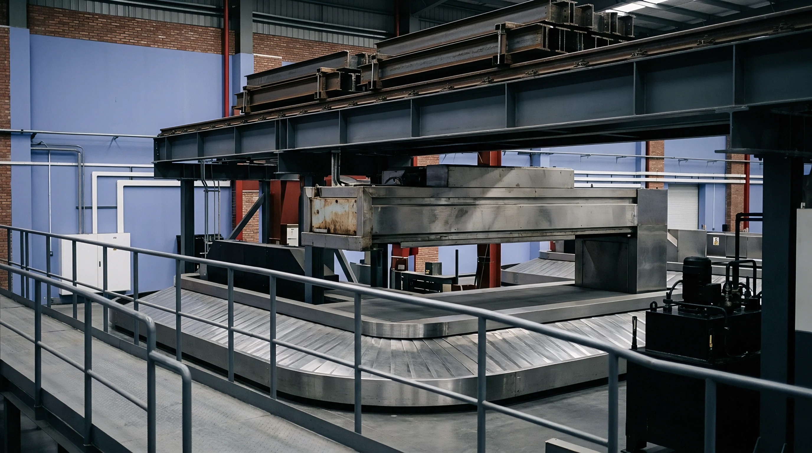
Interdiffusion rates between copper and tin across the Cu3Sn layer operate with severe asymmetry. Copper atoms diffuse outward into the solder matrix significantly faster than tin atoms diffuse inward toward the substrate. This unequal flux generates a net vacancy flow toward the copper substrate, precipitating microvoids along the Cu3Sn/Cu boundary.
These structural cavities are known as Kirkendall voids.
Substrate electroplating chemistry governs vacancy coalescence behavior. Copper plating baths containing excessive organic brighteners, levelers, or sulfur compounds leave codeposited impurities within the copper lattice. During subsequent solid-state aging at elevated temperatures, these impurities segregate to the Cu3Sn/Cu interface, lowering the activation energy for void nucleation.
High-purity rolled annealed copper foils exhibit near-zero Kirkendall void generation, whereas low-tier acid copper baths with uncontrolled additive breakdown products produce continuous planar arrays of voids.
The operational risk materializes during drop impact, vibration, or mechanical shock testing. Under high strain rates, stress concentrations track the perforated Cu3Sn/Cu interface rather than dissipating plastically through bulk solder. Interfacial brittle fracture occurs at shock energy levels sixty percent lower than baseline values.
Assemblies subjected to drop shock requirements fail IPC/JEDEC JESD22-B111 compliance testing when copper plating impurity levels exceed 50 parts per million sulfur or 100 parts per million carbon.
Phase transformation within the Cu6Sn5 compound adds internal mechanical strain. At 186 degrees Celsius, stoichiometric Cu6Sn5 shifts from a high-temperature hexagonal crystal structure to a low-temperature monoclinic structure. This allotropic transformation produces an internal volumetric expansion of approximately 2.15 percent.
Repeated thermal cycling across this transition temperature initiates microcracks within the scallops, accelerating crack propagation through adjacent solder joints under thermal-mechanical fatigue loading.


Finish
Surface finishes serve as sacrificial wetting layers and diffusion barriers to regulate intermetallic development. The selection of surface finish dictates whether the primary intermetallic compound forms as a tin-copper or tin-nickel phase, fundamentally altering interfacial integrity, dissolution velocity, and storage shelf-life. Standard printed circuit board manufacturing deploys organic solderability preservatives, immersion tin, immersion silver, and nickel-based electroplated or electroless coatings.
Organic Solderability Preservative (OSP) coats bare copper with an organometallic chemical film measuring 0.2 to 0.5 micrometers. During reflow, flux acids dissolve the protective film, presenting naked copper directly to molten tin. The resulting reaction produces clean Cu6Sn5 intermetallic scallops with no secondary boundary interfaces.
OSP boards cannot survive multiple thermal passes; second-side reflow and wave rework operations suffer from oxidized copper, poor wetting fillets, and dewetting on large thermal ground lands.
Electroless Nickel Immersion Gold (ENIG) deposits 3.0 to 5.0 micrometers of electroless nickel phosphorus (7 to 10 weight percent phosphorus) topped by 0.05 to 0.1 micrometers of immersion gold. Gold dissolves into molten solder within milliseconds, leaving liquid tin to react directly with the underlying nickel layer. Nickel dissolves into liquid SAC305 at roughly one-thirtieth the rate of pure copper, suppressing substrate erosion and forming a uniform, planar Ni3Sn4 intermetallic layer.
The nickel phosphorus barrier preserves base copper from dissolution, rendering ENIG suitable for fine-pitch Ball Grid Array (BGA) components and multi-stage assembly routines.
Nickel dissolves into molten SAC305 at approximately one-thirtieth the rate of pure copper, establishing ENIG and ENEPIG finishes as effective diffusion barriers for multiple thermal passes.
Electroless Nickel Electroless Palladium Immersion Gold (ENEPIG) introduces an intermediate palladium layer of 0.05 to 0.15 micrometers between the nickel and gold. Palladium acts as a secondary buffer, retarding nickel dissolution while eliminating hyper-corrosion defects during gold immersion. Solder joints on ENEPIG develop a complex (Pd,Ni)Sn4 or (Cu,Ni)6Sn5 compound structure, yielding high shear strength and stable drop-shock performance across extreme automotive thermal bands.

Immersion Surface Topologies and Thinning Limits
Immersion Tin (ImSn) finishes deposit 0.8 to 1.2 micrometers of pure tin directly onto copper via a displacement reaction. Solid-state intermetallic compound formation begins immediately in storage at ambient conditions. Within six months of warehouse exposure at 25 degrees Celsius and 60 percent relative humidity, up to 0.4 micrometers of the tin layer converts into Cu6Sn5.
Thin immersion tin coatings measuring under 0.7 micrometers consume the unreacted tin completely, exposing brittle intermetallic to the atmosphere and causing severe wetting failure during assembly.
Immersion Silver (ImAg) provides a metallic finish of 0.15 to 0.4 micrometers. Silver dissolves rapidly into bulk solder without participating directly in interfacial intermetallic growth, allowing solder to react with the underlying copper to yield Cu6Sn5. Exposure to airborne sulfur compounds in industrial manufacturing zones generates silver sulfide tarnish, producing localized non-wetting or micro-voiding beneath BGA balls.
ImAg surfaces require strict moisture barrier bag packaging with active desiccant and sulfur scavengers.
Direct immersion gold finishes without nickel barriers present catastrophic dissolution dynamics. Gold dissolves instantaneously, followed by rapid, unrestricted copper dissolution into the solder joint. Thin finishes lack barrier capacity, concentrating thermal stress across the primary copper boundary.
Process specifications for high-reliability assemblies prohibit thin non-barrier coatings on multi-pass thermal boards.


Trench
Electroless nickel plating processes harbor a failure mode known as black pad defect. The condition originates during the immersion gold displacement reaction when galvanic hyper-corrosion attacks the underlying electroless nickel-phosphorus deposit. Accelerated nickel dissolution leaves behind a deeply cracked, porous nickel layer enriched with brittle phosphorus (exceeding 12 weight percent phosphorus), capped by thin, discontinuous gold plating.
Solder cannot wet the oxidized, hyper-corroded nickel network.
Under mechanical stress or thermal fatigue, the joint fractures along the compromised nickel boundary with minimal energy absorption. The fracture surface exhibits a dark, mud-crack pattern visible under scanning electron microscopy. Because gold dissolution occurs during reflow while wetting fails at the corroded nickel interface, components pop off circuit boards under minor handling shock or in-circuit testing, showing zero solder fillet adhesion to the surface mount pad.
Root causes track chemical imbalance and bath loading in PCB fabrication facilities. Excessive gold bath acidity (pH below 4.2), elevated bath temperatures, high gold concentrations, and extended immersion dwell times accelerate the corrosion rate of the nickel layer. Sub-optimal hypophosphite control in the nickel bath produces phosphorus-lean micro-domains that corrode preferentially under galvanic drive.
Low pad-to-panel surface area ratios drive galvanic over-activation on isolated SMT pads, concentrating corrosion pits into deep intergranular fissures.
Detecting black pad before component placement requires rigorous incoming quality control protocols. Visual inspection under optical microscopes cannot identify corrosion fissures beneath unbroken immersion gold. Fabricators must cross-section test coupons and perform automated solderability tests across production lots.
Solderability dip-and-look testing per J-STD-003 reveals non-wetting or pinhole de-wetting on affected panels before surface mount placement commences.

Cross-Section Verification and Energy Dispersive Spectroscopy
Standard destructive verification requires metallurgical cross-sectioning through isolated BGA lands followed by scanning electron microscopy (SEM) and energy-dispersive X-ray spectroscopy (EDS). Cross-sections must avoid aggressive polishing abrasives that smear soft gold over brittle corrosion fissures. Low-speed diamond sawing followed by sequential polishing down to 0.05-micrometer colloidal silica exposes intact nickel-phosphorus interfaces.
EDS elemental line scans across the nickel-to-solder interface map phosphorus concentration spikes. A normal electroless nickel layer carries between 7 and 9 weight percent phosphorus. In a black pad condition, hyper-corrosion leaches nickel metal, leaving behind an intermediate layer known as the nickel-rich black band where phosphorus concentration reaches 11 to 14 weight percent.
This hyper-phosphorus layer cannot form a cohesive Ni3Sn4 intermetallic network, precipitating catastrophic joint separation under vibrational strain.
High-speed shear testing and cold bump pull testing serve as mechanical verification methods for incoming bare boards. Solder spheres composed of SAC305 are reflowed onto sample pads and pulled to failure at velocities exceeding 100 millimeters per second. Ductile fracture through the bulk solder ball confirms robust interfacial bonding.
Brittle fracture along the pad-solder interface at low peak force indicates black pad corrosion or excessive phosphorus segregation, demanding immediate containment of the entire PCB production batch.


Doping
Microalloying modifications in lead-free solder matrices alter dissolution rates and control intermetallic layer morphology. Adding precise fractions of transition metals or rare earth elements modifies chemical potentials and diffusion barriers across the liquid-solid interface. The industry relies heavily on additions of nickel, bismuth, cobalt, antimony, and germanium to standard tin-silver-copper and tin-copper formulations to suppress rapid substrate loss.
Doping standard SAC alloys with 0.05 to 0.10 weight percent nickel slows copper dissolution during wave soldering by up to fifty percent. Nickel atoms partition preferentially into the liquid-solid reaction zone, transforming the coarse, scalloped Cu6Sn5 phase into a continuous, fine-grained (Cu,Ni)6Sn5 hexagonal intermetallic layer. This mixed ternary compound acts as a superior diffusion barrier compared to binary Cu6Sn5, retarding the passage of copper atoms into bulk molten tin.
Commercial alloys such as SN100C (Sn-0.7Cu-0.05Ni+Ge) exploit this mechanism to stabilize wave soldering operations.
Germanium additions between 0.005 and 0.01 weight percent act as oxygen getters in molten solder. Germanium migrates rapidly to the liquid surface, forming an ultra-thin germanium oxide film that suppresses dross formation by up to seventy percent at 260 degrees Celsius. In the absence of heavy surface oxide films, liquid surface tension remains uniform, improving dynamic wetting angles on bare copper and reducing mechanical drag during board exit from wave plumes.
Bismuth additions between 1.0 and 3.0 weight percent lower the alloy liquidus temperature, refine the bulk tin grain structure, and enhance mechanical yield strength through solid-solution strengthening. Bismuth atoms do not participate directly in interfacial intermetallic compound formation, remaining dissolved within the bulk beta-tin matrix. In assemblies where components carry legacy tin-lead finishes, bismuth additions must remain below 1.5 weight percent to prevent the formation of a ternary Sn-Pb-Bi eutectic phase that melts at 98 degrees Celsius, destroying joint integrity during operational thermal excursions.

Interfacial Morphology Modification under Doping
Cobalt doping at 0.02 to 0.05 weight percent produces thin, uniform intermetallic compound layers at the copper boundary. Cobalt substitutes for copper within the Cu6Sn5 lattice, forming (Cu,Co)6Sn5. This phase suppresses the formation of the planar Cu3Sn compound during subsequent solid-state thermal aging, directly eliminating the vacancy imbalances that generate Kirkendall voiding.
Drop-shock survival lifetimes for BGA joints increase significantly when cobalt doping stabilizes the copper-solder boundary.
Antimony doping between 0.2 and 0.5 weight percent stabilizes the beta-tin lattice against allotropic transformation into alpha-tin gray powder at low temperatures, a phenomenon known as tin pest. Antimony provides solid-solution strengthening without increasing the melting point excessively. Solder joints operating in sub-zero aerospace and telecommunications environments maintain structural elasticity and resist intergranular fatigue cracking when microalloyed with antimony.
The operational compromise in microalloyed baths centers on composition management. Elements added at low concentrations (under 0.05 weight percent) deplete rapidly through oxidation and intermetallic dross precipitation. Wave solder pots require weekly spectrographic tracking to replenish fugitive elements.
When cobalt or nickel concentrations drop below critical thresholds, dissolution rates revert to uninhibited binary tin-copper levels, catching factory personnel unaware.


Drift
Long-term reliability of lead-free solder interconnects degrades under thermal aging, mechanical vibration, and continuous operational strain. As assemblies age, solid-state intermetallic growth continues at rates governed by the operating temperature of the end device. In consumer computing, automotive electronics, and telecom infrastructure, internal dissipation drives sustained temperatures between 70 and 105 degrees Celsius, shifting interfacial morphology from ductile metal to brittle intermetallic structures.
The continuous growth of interfacial intermetallic compounds consumes the underlying copper trace or pad. On high-density interconnect (HDI) boards featuring microvias, target pad copper thickness frequently measures less than 12 micrometers. Solid-state reaction over ten years of continuous thermal exposure consumes between 3 and 5 micrometers of this copper base to feed expanding Cu6Sn5 and Cu3Sn intermetallic layers.
Microvia target pads experience severe thinning, precipitating barrel-to-target separation and intermittent circuit opening during thermal-mechanical cycling.
Electromigration compounds interfacial drift under high current densities exceeding 10,000 amperes per square centimeter, typical in micro-BGA bumps and power module interconnects. Electron wind forces drive the migration of metal atoms toward the anode, leaving void clusters at the cathode. In lead-free joints, copper from the cathode pad dissolves rapidly into the solder matrix under electrical bias, migrating toward the anode where it precipitates as massive intermetallic crystals.
The cathode interface suffers rapid de-wetting, structural vacancy growth, and premature open-circuit failures.
Thermal fatigue cycling induces strain along grain boundaries within the bulk solder joint. Lead-free alloys exhibit strong elastic and thermal expansion anisotropy across individual body-centered tetragonal beta-tin grains. As temperature cycles between minus 40 and 125 degrees Celsius, adjacent tin grains expand and contract at different rates along their crystallographic axes.
The resulting shear stresses concentrate along the rigid, non-compliant intermetallic compound interface, initiating fatigue cracks that propagate through the brittle intermetallic scallops.

What Drives Interfacial Creep Rupture over Time?
Thermal-mechanical stress profiles accelerate creep deformation in the bulk solder adjacent to the intermetallic boundary. Bulk lead-free solders operate at high homologous temperatures (T / Tm exceeding 0.6) even at room temperature, making continuous plastic deformation and steady-state creep the dominant strain accommodation mechanisms. As intermetallic compounds thicken, the stress field cannot distribute across a ductile boundary, focusing plastic strain into a narrow solder shear band immediately above the intermetallic scallops.
Crack propagation paths shift fundamentally as interfacial compounds mature. In newly formed joints with an intermetallic thickness under 1.5 micrometers, dynamic shear failures shear plastically through bulk solder, demonstrating high energy absorption. When total intermetallic thickness exceeds 4.0 micrometers, crack propagation paths relocate into the brittle intermetallic compound layers or along the Kirkendall voided Cu3Sn/Cu boundary.
Interfacial catastrophic rupture occurs without preliminary plastic yielding, causing sudden field failures in mission-critical environments.
Failure analysis protocols require precise destructive metallurgical preparation to differentiate creep rupture from manufacturing assembly defects. Dye-and-pry testing per IPC-9701 maps fracture propagation across component pin arrays, exposing brittle interfacial separation patterns. Assemblies must undergo thermal shock testing (minus 55 to 125 degrees Celsius, 1,000 cycles) and continuous vibration testing to qualify assembly integrity before releasing production lots to field deployment.

Protocol
Controlling substrate dissolution and intermetallic growth requires strict governance across PCB fabrication, component procurement, assembly thermal profiling, and chemical bath maintenance. A baseline quality plan establishes process parameters, inspection cadences, and analytical testing frequencies to prevent interfacial defects before hardware ships. Factory operations require rigid enforcement of standard procedures across every production shift.
Thermal profiling on surface mount assembly lines must limit total time above liquidus (TAL) while guaranteeing complete solder fillet wetting. Profiling requirements mandate TAL limits of 45 to 75 seconds for SAC305 reflow, with peak package body temperatures held between 235 and 245 degrees Celsius. Extended TAL beyond 90 seconds accelerates copper pad dissolution by forty percent, generating excessively thick initial intermetallic compounds and initiating void nucleation sites before the board leaves the surface mount facility.
Wave and selective soldering operations enforce rigorous copper concentration controls through scheduled chemical titration and replenishments. Process engineers log daily pot throughput, monitoring copper build-up against strict operating thresholds.
- Chemical Spectrometry Analysis verifies alloy composition every 100 operating hours using inductively coupled plasma optical emission spectrometry to track copper, iron, and contamination limits.
- Pot Dilution Flushing introduces pure tin or low-copper replenishment bars whenever bulk copper concentrations reach 0.85 weight percent to restore original alloy fluidity.
- Nitrogen Inerting Blanketing maintains oxygen concentrations below 50 parts per million across the molten wave surface to suppress dross formation and prevent surface tension degradation.
- Solder Immersion Calibration restricts wave contact dwell time between 2.5 and 3.5 seconds using motorized wave-depth gauges to minimize thermal shock and copper erosion.
Inspection regimes must catch sub-surface degradation that automated optical inspection cannot observe. SMT assembly facilities install automated X-ray inspection (AXI) calibrated to detect interfacial voiding exceeding 15 percent total area beneath BGA balls. Boards failing AXI limits undergo non-destructive acoustic microscopy to identify delamination along component substrate pads.
Standard operating procedures must govern PCB supplier qualification and chemical process auditing. Procurement specifications require printed circuit board vendors to submit monthly microsection metallurgical reports showing intermetallic thickness and plating purity. Incoming board lots receive destructive testing to guarantee compliance with international industry standards.
- Verify bare board surface finish thickness across three production panels per lot using X-ray fluorescence spectrometry calibrated against certified standards.
- Conduct cross-sectional metallurgical examination of plated through-holes to confirm copper knee thickness exceeds 18 micrometers and shows zero barrel micro-cracks.
- Execute high-speed cold bump pull testing on sample SMT pads at 100 millimeters per second to verify ductile fracture modes across bulk solder.
- Perform solderability dip-and-look testing per J-STD-003 after eight hours of accelerated steam aging to confirm wetting retention across storage intervals.
- Issue formal supplier containment notices and halt production lot release immediately if cross-sectional analysis reveals interfacial hyper-corrosion, black pad micro-cracking, or phosphorus concentrations exceeding 11 weight percent.
Long-term commercial contracts govern supplier liability regarding latent interfacial defects. Standard procurement terms incorporate IPC-6012 Class 3 performance standards and define clear warranties covering mechanical joint integrity under field operations. PCB fabricators must maintain bath chemistry logs for a minimum of three years to ensure full material traceability in the event of systemic field failures.