Meaning
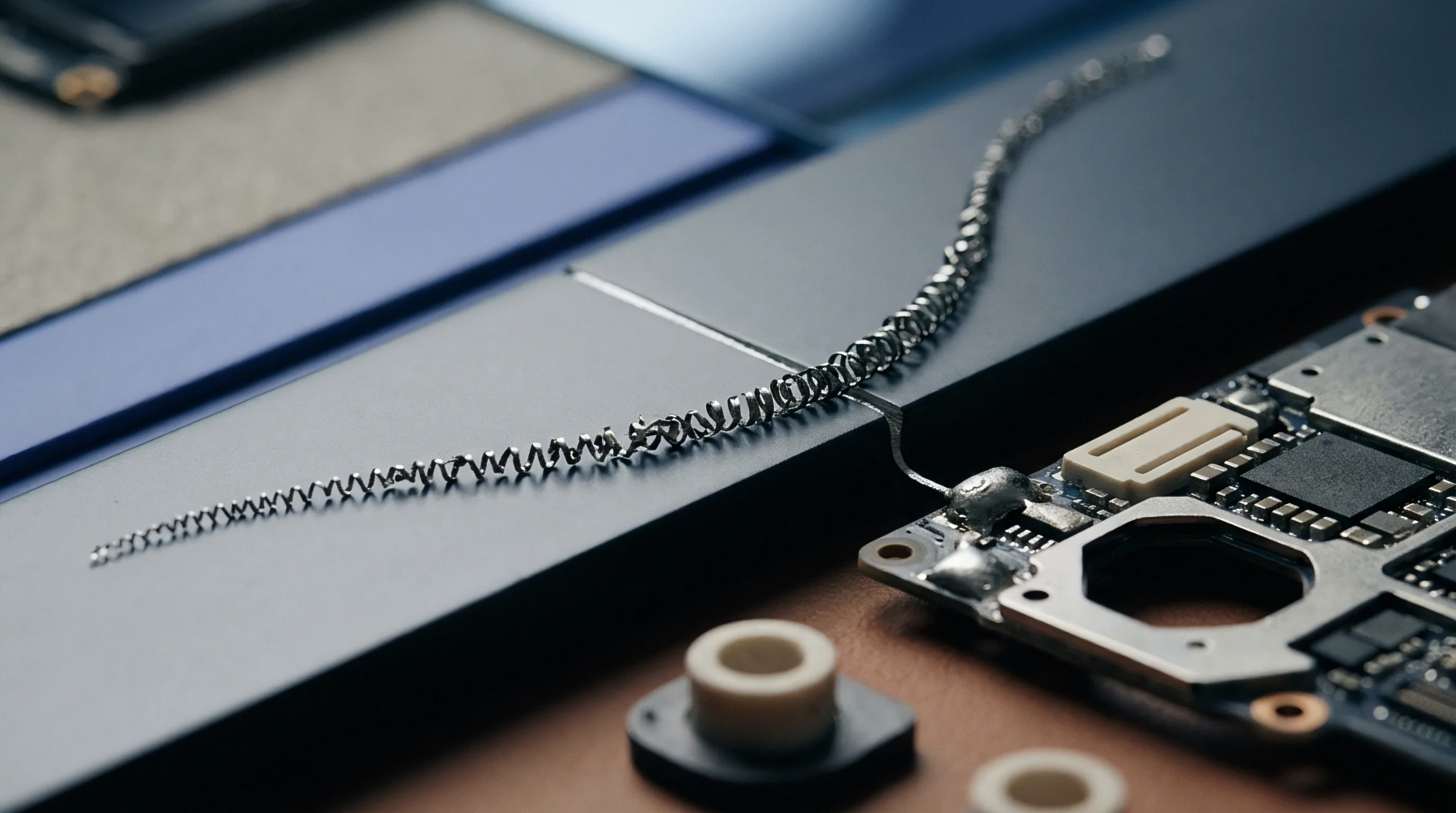
Crystalline substance forms between different metal elements during the soldering process and provides the essential metallurgical bond between the component and the circuit board. This intermetallic compound is a unique material that has a fixed atomic ratio and properties that differ significantly from its parent metals. In the manufacturing sector of mainland China, the formation and growth of these compounds are the primary factors that determine the strength and reliability of electronic assemblies.
While a thin layer is necessary for a stable connection, excessive growth can lead to brittleness and premature failure of the joint. Engineers must carefully control the reflow process to ensure the resulting bond has the optimal microstructure for its intended application.
Structural Formation
Molten solder reacts with the solid copper pads on a printed circuit board to create a layer of new crystals at the interface of the two materials. This intermetallic compound begins to grow the moment the solder reaches its liquidus temperature, with tin atoms diffusing into the copper to form structures like eta phase or epsilon phase. The morphology of these crystals, often appearing as scallops or needles, determines how well the joint can withstand mechanical stress.
A uniform and continuous layer is the hallmark of a high quality soldering process, indicating that the surfaces were properly cleaned by the flux and that the temperature was sufficient for bonding. Quality control technicians use cross sectional analysis and scanning electron microscopy to verify the internal structure of the joints. This detailed inspection is a standard part of the qualification process for any new production line.
Joint Strength
Mechanical properties of an electronic assembly are directly tied to the thickness and stability of the crystalline layers at the interface. An intermetallic compound is inherently harder and more brittle than the surrounding solder or the copper substrate. If the layer is too thin, the joint may lack the necessary adhesion to stay attached under stress.
Conversely, a layer that is too thick creates a brittle path where cracks can easily form and propagate, leading to a sudden and catastrophic break. This balance is especially critical for products used in high vibration environments like aerospace or heavy industry. Manufacturers in the electronics hubs of the Yangtze River Delta optimize their reflow profiles to keep the intermetallic thickness within a specific range, usually between one and five micrometers.
Achieving this target ensures that the joint has enough strength to be reliable without being so brittle that it fails during handling.
Long-term Reliability
Evolution of the crystalline interface continues throughout the life of an electronic device, especially when it is operated at elevated temperatures. The intermetallic compound layer will thicken over time as diffusion continues, potentially consuming the entire copper pad or changing into a more brittle phase. This growth can eventually lead to the formation of voids and the loss of electrical conductivity, a common cause of failure in older electronics.
Reliability testing involves subjecting samples to hundreds of thermal cycles and thousands of hours of high temperature storage to simulate the aging process. These tests help manufacturers predict how long their products will last in the field and set appropriate warranty periods. Understanding the long term behavior of these compounds is a requirement for any firm seeking to compete in the global market for high quality electronics.
The final design must account for these changes to ensure the product remains safe and functional for its entire service life.