
Arrhenius Solid State Diffusion Parameters for Lead Free PCB Surface Finishes
Solid-state diffusion parameters dictate lead-free PCB surface finish shelf life, intermetallic growth, and solder joint reliability under thermal exposure.
Solid-state diffusion parameters dictate lead-free PCB surface finish shelf life, intermetallic growth, and solder joint reliability under thermal exposure.

Controlling interfacial intermetallic growth requires optimizing reflow profiles, selecting microalloyed solder alloys, and auditing substrate copper plating quality.

Thermal aging accelerates SAC305 intermetallic growth through parabolic diffusion, where Cu3Sn layer thickening and Kirkendall voiding reduce joint shear strength.

Thermal aging validation of fine pitch solder joints requires argon ion milling and low-voltage FE-SEM to distinguish genuine submicron Kirkendall voids from mechanical polishing artifacts before enforcing contractual lot rejection criteria.
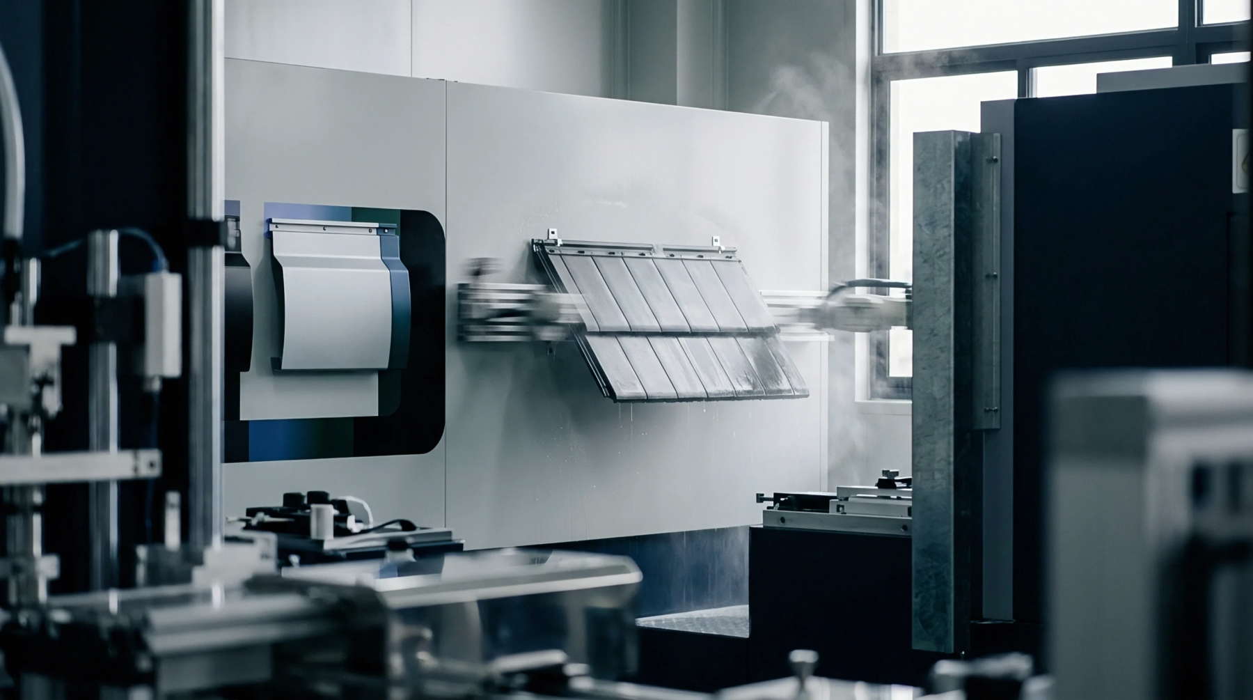
Control reflow peak dwell and solid-state thermal exposure to limit interfacial intermetallic growth below four micrometers, preventing brittle joint fracture.

Quantifying interfacial intermetallic growth kinetics under thermal aging enables accurate interconnect lifetime predictions and prevents field failures.
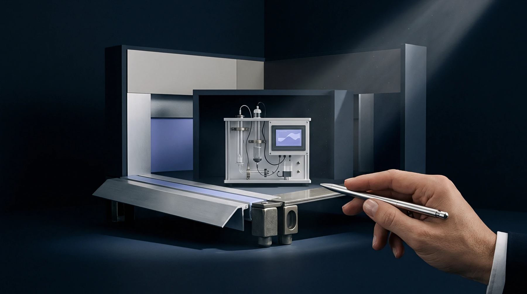
Managing lead-free solder intermetallic growth requires strict reflow thermal limits to prevent brittle phase formation and latent interfacial field failures.

Lead-free solder microstructures coarsen rapidly under thermal heat, requiring micro-alloying and strict reflow oversight to stop intermetallic failures.

Excessive intermetallic layer growth and Kirkendall voiding cause brittle solder joint field failures that require precise contractual latent defect rules.

Solid-state intermetallic growth follows parabolic diffusion kinetics governed by Arrhenius thermal activation, requiring barrier finishes like ENIG or ENEPIG to limit brittle interface thickening and prevent Kirkendall void failures in extended service.

Controlling lead-free interfacial IMC growth demands peak reflow temperatures below 245 degrees Celsius and strict limits on total dwell time above liquidus.
Lead-free solder intermetallic layer growth follows parabolic solid-state diffusion kinetics, requiring strict reflow temperature control and micro-alloying to prevent embrittlement.

Microvoid nucleation at copper surface finish interfaces stems from electroplating bath impurity co-deposition accelerating solid-state vacancy condensation.

Control reflow liquidus dwell and thermal aging exposure to restrict brittle interfacial compound growth and eliminate Kirkendall microvoiding failure paths.

Thermal aging drives intermetallic growth and Kirkendall voiding in lead-free interfaces; controlling copper pad purity and reflow profiles prevents brittle failure.
Accurate intermetallic growth measurement requires targeted chemical etching, calibrated SEM imaging, and Arrhenius diffusion kinetic modeling.
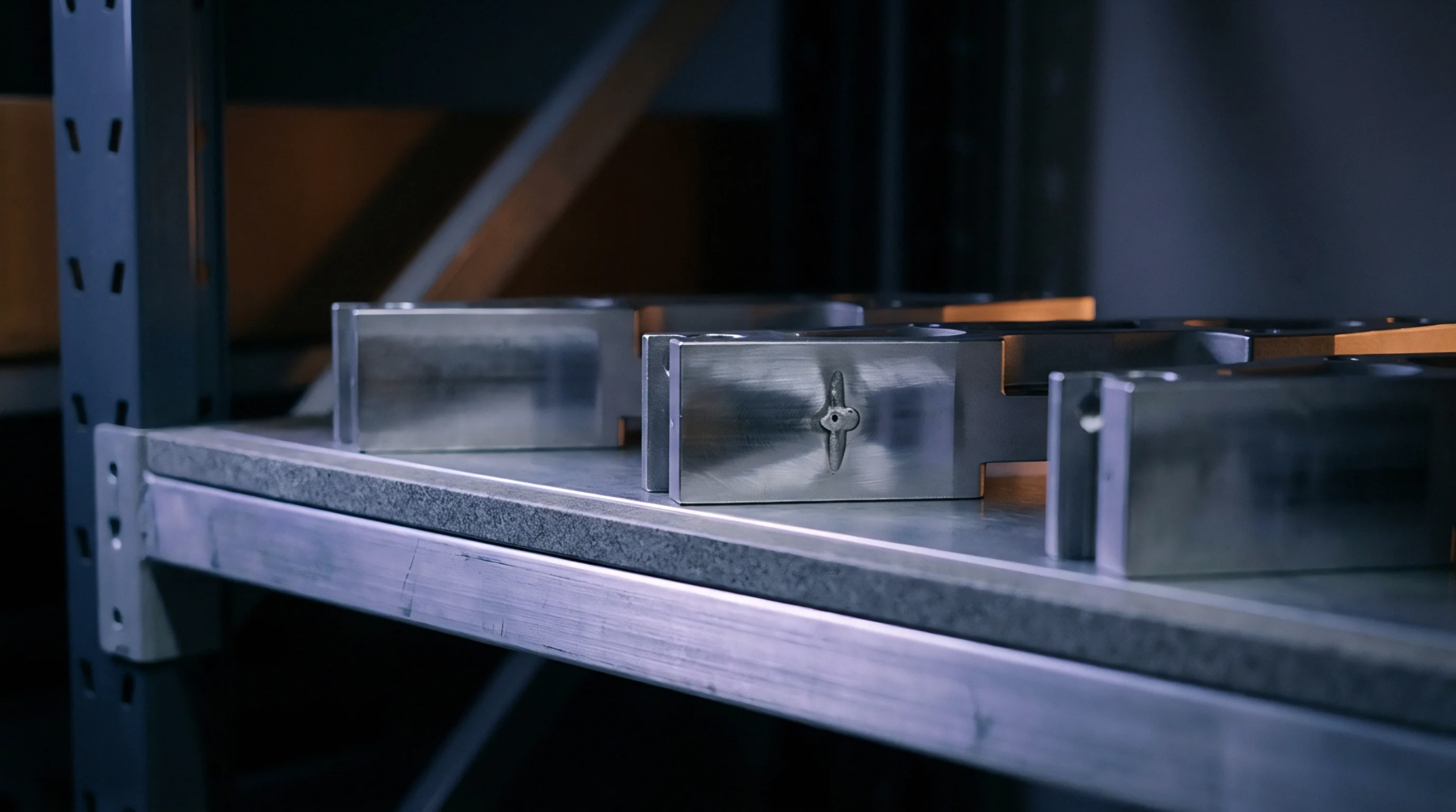
Doping tin-based solders with trace nickel, cobalt, or zinc alters interdiffusion kinetics, suppressing Kirkendall voiding and securing long-term joint strength.

Quantifying lead-free solid-state diffusion requires Arrhenius aging matrices to enforce 4.0-micrometer IMC limits and suppress brittle failure risks.

Post-holiday wave solder joints require ICP bath assays and high-speed shear testing to detect latent intermetallic embrittlement before field failure.
Expertise is a utility, not a secret. sentiention™ publishes its working knowledge as open reference: intelligence layer covering the materials it sources, the markets it enters, and the reference that serves both.