Intermetallic Growth Kinetics in Lead Free Reflow Assembly
Reflow thermal exposure dictates initial intermetallic thickness, where excess heat accelerates Kirkendall voiding and brittle interfacial joint rupture.
Boundary
A cross-section polished to 0.05-micron colloidal silica reveals whether twenty seconds of excessive heat converted ductile solder into a brittle joint. Molten SAC305 alloy (96.5 percent tin, 3.0 percent silver, 0.5 percent copper) dissolves copper metallization at rates exceeding 0.1 microns per second at 240°C. Tin dissolves copper rapidly. This chemical affinity drives instantaneous dissolution followed by the precipitation of intermetallic compound crystals along the liquid-solid dividing line.
The composition and geometry of this interfacial region determine whether an assembly survives standard operational vibration or cleaves under moderate drop shock.
Lead-free solders run hotter than legacy tin-lead eutectic systems. The higher processing temperatures, centered between 235°C and 255°C, accelerate copper erosion and expand the resulting compound band. The reaction layer displays a scallop morphology during initial reflow.
Molten solder flows between these scalloped hummocks, feeding liquid tin directly to the fresh copper boundary. Intermetallic growth during liquidus exposure is governed by chemical dissolution and fast interfacial reaction rather than slow solid-state lattice diffusion.
Peak reflow temperatures above 245°C held beyond sixty seconds expand interfacial Cu6Sn5 scallop thickness past 1.6 micrometers on bare copper pads.
The morphology changes during solidification. The scallop valleys fill as the molten pool recedes, leaving an irregular band dominated by copper-tin phases. The initial thickness of this layer establishes the baseline mechanical state of the solder interconnect.

Liquidus Dissolution Rates
Molten lead-free alloys attack copper substrates the moment furnace temperatures exceed 217°C. The dissolution rate constant follows an Arrhenius relationship driven by liquid-phase mass transport. At 230°C, bare copper dissolves into liquid SAC305 at approximately 0.08 microns per second, rising to 0.15 microns per second at 250°C. Solder volume limits this reaction: once local copper saturation reaches 1.2 weight percent in the liquid joint, chemical dissolution decelerates, shifting the mechanism toward intermetallic scallop ripening.
Liquid solder pulls copper inward. Scallop ripening occurs through Ostwald ripening kinetics, where larger Cu6Sn5 scallops grow at the expense of adjacent smaller grains through channels of liquid solder separating the crystalline domes. The average scallop radius grows proportional to the cube root of the time above liquidus.
Prolonged liquidus dwelling creates coarse, continuous intermetallic bands with deep grain boundary grooves. These grooves act as microstructural stress concentrators under mechanical loading.

Interfacial Phase Sequence
Chemical reactions along the contact zone yield distinct stoichiometric compounds before the printed circuit board leaves the reflow peak. The thermodynamic driving force favors the rapid nucleation of eta-phase Cu6Sn5 immediately adjacent to the molten solder.
- Eta-phase Cu6Sn5 precipitates first as elongated scallop structures extending directly into the solder matrix, displaying a hexagonal crystal structure at reflow temperatures that transforms to a monoclinic superlattice upon cooling below 186°C.
- Epsilon-phase Cu3Sn develops between the Cu6Sn5 layer and the copper pad as an ultra-thin planar band, sustained by copper diffusion through the initial intermetallic crystal lattice.
- Ternary (Cu,Ni)6Sn5 forms on nickel-plated pads, incorporating nickel atoms into the crystal lattice and slowing compound layer growth by fifty percent compared to bare copper.
- Silver-tin Ag3Sn precipitates as discrete plate-like crystals within the bulk solder near the intermetallic boundary, occasionally forming large needle structures when cooling rates drop below 1.5°C per second.
Silver forms silver-tin plates. Excessive accumulation of plate-like Ag3Sn structures adjacent to the interfacial scallops creates cleavage planes that separate under mechanical shear. The mechanical performance of the joint depends upon limiting the initial total compound thickness below two micrometers during the primary thermal excursion.

Furnace
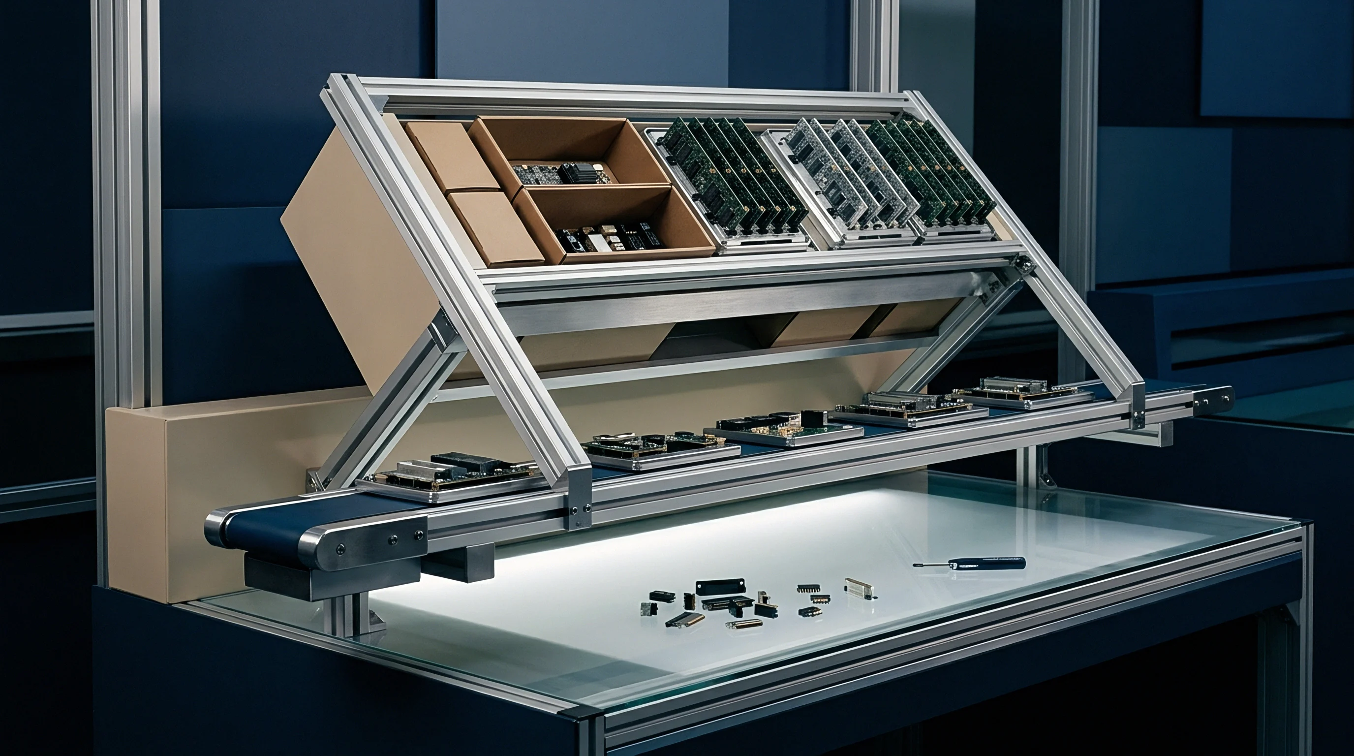
Conveyor speed settings and ten-zone heating profiles determine the total thermal dosage delivered to every surface mount component. Thermal dosage represents the integral of temperature over time above the alloy melting threshold. In high-density printed circuit board assembly, component mass variance creates substantial temperature differentials across a single board.
Small passive components reach peak temperatures twelve to fifteen degrees higher than large ball grid array packages, creating localized zones of accelerated intermetallic growth.
Faster furnace conveyor speeds reduce thermal exposure but create uneven solder paste dissolution across high-density board assemblies.
Solder paste flux activates within the preheat window between 150°C and 190°C, stripping native copper oxides to enable spontaneous wetting. Excessive exposure in this zone exhausts activator chemistry before the solder paste particles melt. The reflow segment requires exact conveyor timing to balance complete wetting against intermetallic compound development.
Which Process Variable Dictates Intermetallic Thickness?
Time above liquidus governs compound layer development far more aggressively than peak temperature alone. When time above liquidus extends from 45 seconds to 90 seconds at a constant peak temperature of 245°C, interfacial Cu6Sn5 thickness expands from 1.1 microns to 1.9 microns. Raising the peak temperature from 240°C to 255°C while holding time above liquidus at 50 seconds increases thickness by only 0.25 microns.
Excess heat accelerates scallop ripening. Solder technicians balancing line yield frequently extend dwell times to eliminate cold solder defects on dense ground planes, inadvertently creating overly thick interfacial compounds across smaller components. Controlling the conveyor rate to hold the liquidus window between 45 and 60 seconds provides sufficient wetting while preventing compound growth past 1.5 microns.
| Peak Temperature (°C) | Time Above 217°C (s) | Cooling Rate (°C/s) | Substrate Surface Finish | Initial Cu6Sn5 Thickness (µm) | Initial Cu3Sn Thickness (µm) |
|---|---|---|---|---|---|
| 235 | 45 | 3.0 | Organic Solderability Preservative | 0.85 | 0.15 |
| 245 | 60 | 2.5 | Organic Solderability Preservative | 1.25 | 0.28 |
| 255 | 90 | 1.8 | Organic Solderability Preservative | 1.95 | 0.45 |
| 245 | 60 | 2.5 | Electroless Nickel Immersion Gold | 0.55 | 0.00 |
| 255 | 90 | 1.5 | Electroless Nickel Immersion Gold | 0.92 | 0.00 |
| 245 | 60 | 2.5 | Immersion Silver | 1.18 | 0.22 |

Zone Temperature Management
Ten heating chambers arranged in series provide the thermal graduation needed to activate flux without scorching delicate silicon. Peak reflow occurs in zones eight and nine, where convection blowers force heated nitrogen gas across the board assembly. Nitrogen atmospheres suppress oxidation.
Nitrogen atmospheres with oxygen levels below 500 parts per million enhance solder wetting speeds, allowing engineers to shorten time above liquidus by eight to twelve seconds without risking void formation.
Cooling rates govern grain sizes. The cooling segment in zone ten directly shapes the final intermetallic microstructure. A cooling rate between 2.5°C and 4.0°C per second freezes the molten solder rapidly, arresting the growth of Cu6Sn5 scallops and refining the bulk solder grain structure.
Cooling rates below 1.5°C per second allow continued ripening of the intermetallic scallops and promote the growth of brittle Ag3Sn plates within the bulk joint.
Improper furnace balance yields cumulative thermal damage that degrades joint integrity, forcing the discard of populated board panels during subsequent mechanical screening.

Pore
Solid-state diffusion continues to rearrange copper and tin atoms long after assemblies cool to ambient warehouse temperatures. Operating environments between 80°C and 125°C provide thermal energy that drives solid-state growth of both Cu6Sn5 and Cu3Sn. In this solid-state regime, atomic transport proceeds via vacancy diffusion across crystalline lattices and along grain boundaries.
Copper atoms migrate into the intermetallic layer faster than tin atoms diffuse into the underlying copper metallization.
Unequal diffusion rates generate a net flux of vacancies toward the copper substrate, a phenomenon known as the Kirkendall effect. Vacancies coalesce into micro-voids along the interface between Cu3Sn and the copper pad. High operating temperatures accelerate void formation.
A two-sentence look at maritime history provides context: early twentieth-century naval engineers observed identical vacancy coalescence and dezincification in brass condenser tubes exposed to heated seawater, long before semiconductor packaging encountered planar interface voids. This vacancy coalescence degrades interfacial mechanical strength.

Kirkendall Vacancy Coalescence
Unequal atomic flux rates create empty lattice sites inside the bi-metallic transition region. Copper atoms exhibit a diffusion coefficient approximately three times higher than tin atoms within the Cu3Sn crystal lattice at 125°C. The excess vacancies left behind in the copper lattice migrate toward regions of low free energy, condensing along the planar Cu3Sn/Cu boundary.
Substrate impurities govern void density. Copper electroplating baths containing sulfur-based organic brighteners leave trace sulfur, carbon, and chlorine residues within the deposited foil. These impurity atoms segregate to the Cu3Sn/Cu interface, pinning vacancies and lowering the activation energy for micro-void nucleation.
Under prolonged thermal exposure, isolated micro-voids expand and coalesce into continuous planar voids, severely reducing the effective load-bearing area of the solder pad.
| Intermetallic Phase | Diffusing Species | Pre-Exponential Factor D0 (m²/s) | Activation Energy Q (kJ/mol) | Activation Energy Q (eV) | Kirkendall Void Propensity |
|---|---|---|---|---|---|
| Cu6Sn5 | Tin and Copper | 1.5 × 10⁻⁷ | 78.5 | 0.81 | Negligible |
| Cu3Sn | Copper | 2.8 × 10⁻⁶ | 101.4 | 1.05 | Severe |
| (Cu,Ni)6Sn5 | Copper and Tin | 3.2 × 10⁻⁸ | 92.1 | 0.95 | Low |
| Ni3Sn4 | Tin | 4.1 × 10⁻⁷ | 118.6 | 1.23 | Minimal |
Consider a worked construction comparing thermal aging for Cu3Sn growth across a 1,000-hour dwell time at two operating temperatures. Assume an initial reflow Cu3Sn thickness of 0.30 microns, a pre-exponential factor D0 of 2.8 × 10⁻⁶ m²/s, an activation energy Q of 101.4 kJ/mol, and the ideal gas constant R equal to 8.314 J/(mol·K). The parabolic growth constant D equals D0 multiplied by the exponential of negative Q divided by RT.
At an operating temperature of 100°C (373 Kelvin), RT equals 3.101 kJ/mol. The ratio Q/RT equals 32.70, yielding an exponential factor of 6.30 × 10⁻¹⁵. Multiplying by D0 gives a diffusion coefficient of 1.76 × 10⁻²⁰ m²/s.
Over 1,000 hours (3.6 × 10⁶ seconds), the diffusion distance squared equals 6.34 × 10⁻¹⁴ m², producing a solid-state thickness increase of 0.25 microns. The total Cu3Sn thickness reaches 0.55 microns, leaving the interface largely free of continuous void networks.
At an elevated temperature of 150°C (423 Kelvin), RT rises to 3.517 kJ/mol. The ratio Q/RT drops to 28.83, generating an exponential factor of 3.02 × 10⁻¹³. The resulting diffusion coefficient increases to 8.46 × 10⁻¹⁹ m²/s, an increase of nearly forty-eight times over the 100°C value.
Over the identical 1,000-hour window, the solid-state growth produces a layer increase of 1.74 microns. Total Cu3Sn thickness expands to 2.04 microns. This substantial diffusion flux deposits millions of vacancies along the copper boundary, initiating chain-like Kirkendall void networks.
The activation energy figure of 0.81 eV for Cu6Sn5 growth rests on thin-film diffusion couples tested at 100°C to 170°C under 500-hour dwells, where grain boundary diffusion dominates over lattice diffusion. If tested on bulk single-crystal couples where grain boundaries are absent, the measured activation energy would shift toward 1.20 eV. A specific figure the industry disputes is the exact void area fraction needed to cause field failures.
Many packaging laboratories cite a threshold of 15 to 20 percent void area fraction along the Cu3Sn interface as the critical point for spontaneous drop shock failure. The desk cannot fully defend this 20 percent figure because stress concentration depends heavily on local void clustering and pad geometry rather than total area. Under this uncertainty, a prudent buyer specifies zero continuous micro-void lineation across five cross-sections sampled per lot.

Substrate Barrier Selection
Plating layers applied over bare copper foils reshape diffusion paths during subsequent thermal stress. Surface finishes alter intermetallic reaction kinetics directly.
- Electroless Nickel Immersion Gold deposits three to five microns of nickel phosphorus, serving as a robust physical barrier that impedes copper diffusion and forms ternary (Cu,Ni)6Sn5 compounds.
- Electroless Nickel Electroless Palladium Immersion Gold adds an intermediate palladium layer that prevents nickel corrosion during chemical plating and suppresses interfacial micro-voiding.
- Immersion Silver Finish dissolves completely into the bulk solder within three seconds of reflow, leaving the underlying copper directly exposed to liquid and solid-state diffusion.
- Organic Solderability Preservative volatilizes during reflow without introducing foreign metallic elements into the joint, resulting in standard Cu6Sn5 and Cu3Sn phase formation.
Nickel stalls vacancy migration. An unresolved physical question remains regarding whether trace additions of bismuth or antimony into standard lead-free alloys can alter the chemical potential gradient sufficiently to prevent Kirkendall vacancy condensation over five-year field deployments.


Rupture
Mechanical failure during handling or transit exposes the metallurgical weakness built during thermal processing. Intermetallic compounds possess high elastic moduli but minimal plastic ductility. While bulk SAC305 solder displays an elongation at break exceeding thirty percent, Cu6Sn5 and Cu3Sn intermetallic layers fail at strains below two percent.
When a printed circuit board experiences dynamic bending, strain concentrates within the thin intermetallic zone.
Brittle interfaces fracture cleanly. Solder joints with intermetallic layers thinner than 1.5 microns absorb mechanical shocks through plastic deformation of the ductile bulk solder. Once the intermetallic layer expands beyond 4.0 microns, mechanical shock triggers brittle cleavage fracture along the compound boundary.
Cleavage cracks propagate along the planar boundary separating Cu3Sn from copper under mechanical shock.
The 4.0-micron threshold rests on drop hammer testing of 0.5-millimeter pitch ball grid arrays under 1500g half-sine pulses per JESD22-B111. Reducing solder ball volume or utilizing thinner copper traces shifts this critical threshold down toward 2.8 microns.

High Strain Dynamics
Sudden deceleration forces generate tensile stress waves across every ball grid array attachment. At strain rates exceeding 10¹ s⁻¹, bulk solder cannot relax applied mechanical stress through dislocation creep. The stress transfers directly into the interfacial joint boundary.
High strain rates break joints.
Drop tests expose weak bonds. Evaluating high-strain integrity requires standardized shock impact testing using high-speed data acquisition channels. Technicians evaluate mechanical integrity through a sequence of physical procedures:
- Mount the populated circuit board onto four corner support posts inside a standard drop test fixture.
- Calibrate the drop tower drop height to produce a 1500g peak acceleration with a 0.5-millisecond half-sine duration.
- Connect dynamic resistance monitoring channels across daisy-chained component networks to detect transient electrical interruptions.
- Drop the test fixture repeatedly until electrical resistance spikes exceed 100 ohms for more than 200 nanoseconds.
- Dismount the assembly and cut through failed corner joints using a slow-speed diamond wafering blade.
- Examine the fractured interface under a field emission scanning electron microscope to categorize the failure mode.
Ductile failure produces classic dimpled rupture surfaces within the bulk solder matrix. Interfacial failure produces flat, mirror-like cleavage facets across the intermetallic compound grains.

Cleavage Plane Progression
Cracks initiate at stress concentration notches along the perimeter of the pad before traveling across brittle intermetallic compounds. In joints aged under elevated temperatures, the crack path follows the Kirkendall void plane between the Cu3Sn layer and the copper pad. In unaged boards subjected to excessive reflow dwell times, the crack propagates through the scallop valleys of the Cu6Sn5 layer.
Shear values drop under heat. When challenged regarding brittle pad detachment on incoming board lots, factory managers often claim the component supplier provided oxidized solder spheres that degraded interfacial wetting rather than acknowledging furnace profiling errors.

Gate
Receiving docks demand rigorous verification criteria to prevent compromised circuit boards from reaching downstream enclosure assembly. Relying entirely on surface appearance or automated optical inspection fails to catch latent intermetallic embrittlement. A solder joint can exhibit perfect wetting angles, bright reflective surfaces, and zero solder bridging while harboring a four-micron intermetallic layer pitted with Kirkendall micro-voids.
Physical verification requires sacrificial coupon testing. Metallographic cross-sectioning accompanied by backscattered electron microscopy provides conclusive measurement of intermetallic thickness and phase stoichiometry. Cross-sections reveal true thickness.
IPC-A-610 Section 5 rejects assemblies where dewetting or intermetallic depletion exceeds twenty-five percent of the contact perimeter.
Polishing scratches mask micro-voids. Standard mechanical polishing using aluminum oxide papers often smears soft bulk solder across the intermetallic boundary, obscuring Kirkendall voids under optical microscopes. Accurate assessment requires progressive diamond suspensions down to 0.25 microns, finishing with an active chemical etch to reveal the compound microstructure clearly.

Microsection Inspection Standards
Diamond saws cutting through solder balls reveal the internal layer architecture under optical and scanning electron microscopes. Inspection routines must measure intermetallic thickness at five distinct points across the pad, averaging the values to account for scallop height variation. The total intermetallic thickness on newly manufactured assemblies should remain within 0.8 to 2.0 microns.
Repeated reflow triples intermetallic thickness. Double-sided surface mount boards run through the reflow oven twice, doubling the thermal exposure of the first-pass joints. Rework operations using localized hot gas nozzles deliver severe, uncontrolled thermal spikes that frequently expand intermetallic layers beyond 4.5 microns on adjacent components.

Commercial Allocation of Rework Costs
Supply contracts assign financial responsibility for latent joint degradation discovered after board delivery. Standard manufacturing services agreements frequently exclude latent metallurgical defects, treating field solder fracture as assembly handling damage rather than a process defect.
To eliminate this commercial exposure, buyers incorporate strict thermal profile limits into the manufacturing agreement. The agreement specifies that no delivered assembly may experience more than two reflow cycles, with peak temperatures capped at 248°C and times above liquidus restricted to sixty seconds. IPC J-STD-001 Section 8 specifies criteria for thermal profile qualification, and incorporating this exact clause into purchase order terms allows the buyer to reject lots whose sacrificial coupon cross-sections reveal intermetallic layers exceeding 2.5 microns, shifting complete replacement and screening costs onto the manufacturing partner.