Electroless Nickel Immersion Gold Hyper Corrosion Detection in Board Assembly
Detecting ENIG hyper corrosion requires destructive micro-sectioning and FIB-SEM to identify phosphorus-rich nickel spikes before assembly reflow.
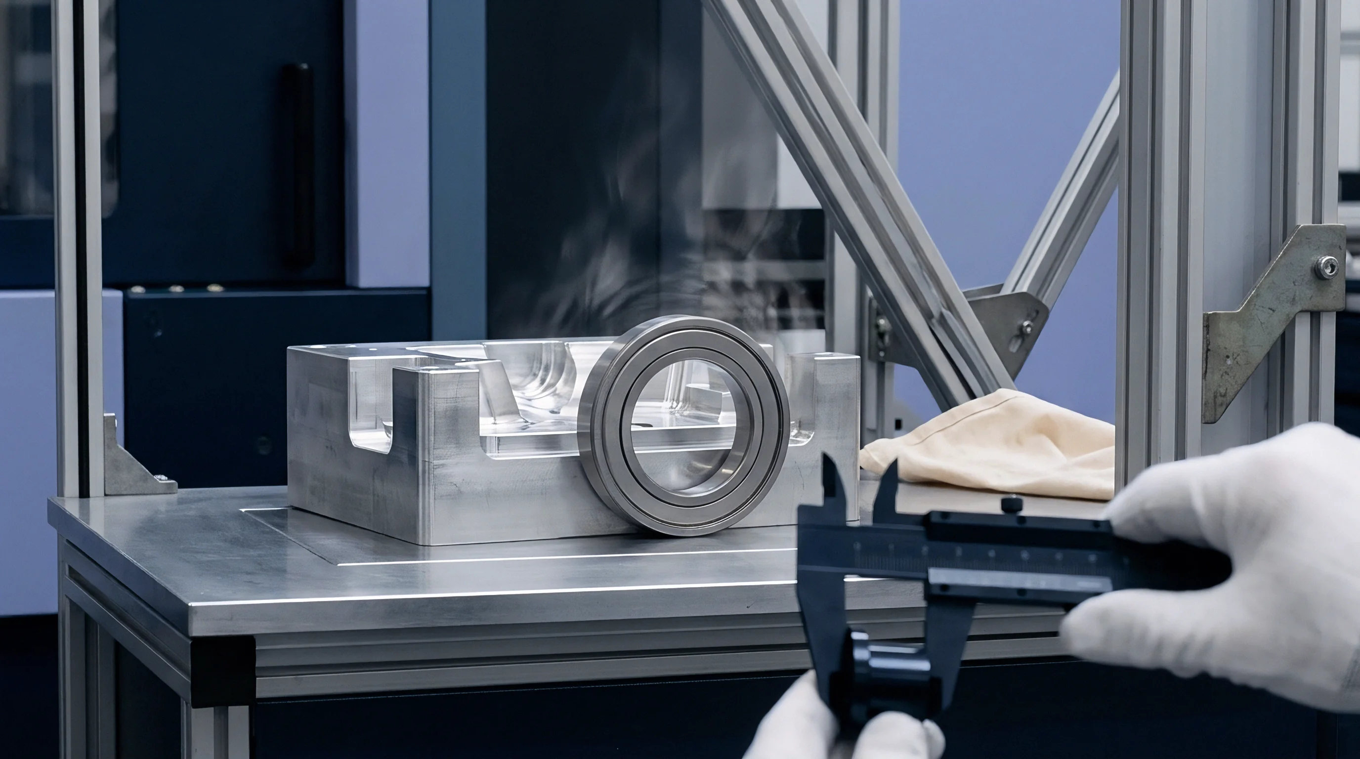

Pore
Deep microscopic trenching within the electroless nickel layer occurs during displacement gold deposition when galvanic attack concentrates at nickel grain boundaries. Electroless Nickel Immersion Gold relies on a two-step chemical process. First, an autocatalytic hypophosphite bath deposits a nickel-phosphorus alloy coating onto exposed copper pads, typically reaching a thickness between three and six micrometers with a phosphorus content of seven to eleven percent by weight.
Second, the board enters an immersion gold bath where metallic nickel transfers electrons to gold ions in solution. Gold precipitates onto the pad while nickel dissolves into the bath. This chemical exchange ideally ceases once a thin, continuous gold film measuring between 0.025 and 0.075 micrometers covers the nickel substrate.
When bath parameters drift, the exchange reaction converts from a uniform surface displacement into aggressive, localized chemical dissolution, driving narrow structural fissures deep into the underlying alloy along vulnerable grain boundaries.
In board assembly, this localized dissolution leads to hyper corrosion, commonly termed black pad, which manifests as narrow, needle-like voids extending vertically through the deposit. Visual inspection cannot catch the defect because the gold overlay bridges across the corrosion trenches, masking severe structural degradation beneath a bright, reflective surface. When assemblies enter surface mount technology lines, molten lead-free solder dissolves the thin gold layer instantly but fails to wet the compromised, highly oxidized nickel underneath.
Solder joint strength then collapses under minor mechanical shear or thermal shock. Catching hyper corrosion before board population demands understanding both the chemical mechanisms driving galvanic attack and the microstructural signatures left behind.

Immersion Gold Displacement Kinetics and Nickel Attack
Galvanic potential differences between freshly deposited metal and underlying phosphorus-rich alloys accelerate localized dissolution during bath immersion. The immersion gold reaction functions purely through galvanic exchange without external electrical current: metallic nickel oxidized at the surface releases two electrons, reducing dissolved gold cyanide complexes to elemental gold. As gold atoms deposit across the surface, they form an initial thin membrane.
If this membrane remains porous or exhibits crystalline vacancies, an electrochemical cell forms. The exposed nickel acts as an anode while the newly deposited gold surface acts as a cathode. Because the surface area of the gold cathode vastly exceeds the small exposed anodic nickel sites inside microscopic pores, local current density at the nickel interface spikes dramatically.
That high current density drives rapid, targeted nickel dissolution directly at grain boundaries where atomic binding energy is lowest. The immersion bath continues stripping nickel from these narrow channels, sending deep structural spikes toward the underlying copper substrate. High bath acidity, low gold metal concentration, and excessive immersion dwell times intensify the attack.
Plating facilities attempting to boost gold thickness on heavy-gold specifications often run immersion cycles past six minutes. Extended immersion forces the bath to seek sub-surface nickel pathways, multiplying the density of hyper-corrosive spikes into a lattice of empty or gold-filled fissures that sever the structural continuity of the nickel pad.
An immersion gold layer measuring below 0.04 micrometers combined with a nickel phosphorus concentration above 10.5 percent by weight reduces intermetallic shear resistance by 62 percent after two reflow cycles.
Phosphorus Enrichment Bands and Microstructural Failure
Chemical dissolution during immersion gold plating strips elemental metal while leaving elemental phosphorus behind at the interface. Electroless nickel deposits consist of a metastable nickel-phosphorus alloy matrix. When the immersion gold bath selectively dissolves metallic nickel atoms, phosphorus cannot enter the gold crystal structure nor easily dissolve into the plating solution.
Phosphorus atoms accumulate along corrosion interfaces, forming an amorphous, highly reactive layer enriched with nickel phosphide phase structures. This enriched band, often reaching phosphorus concentrations exceeding fifteen weight percent, exhibits extreme brittleness and high electrical resistivity.
The boundary between the bulk electroless nickel and the phosphorus-enriched hyper-corroded zone creates a natural fracture line. Under mechanical deflection, vibration, or thermal expansion stress, micro-cracks propagate rapidly along this phosphorus-rich interface. IPC-4552B standards categorize hyper corrosion severity into three distinct structural classifications based on cross-sectional examination:
- Level 1 Dissolution Shallow surface depressions extending less than twenty percent into the total electroless nickel deposit thickness, presenting isolated corrosion spikes without continuous intercrystalline trenching across the pad surface.
- Level 2 Dissolution Moderate intercrystalline attack penetrating between twenty and forty percent of the nickel deposit thickness, accompanied by visible phosphorus accumulation along primary grain boundaries without complete pad separation.
- Level 3 Hyper Corrosion Severe, deep corrosion spikes penetrating beyond forty percent of the total nickel deposit thickness, forming extended continuous bands of phosphorus-enriched nickel residue across more than thirty percent of the pad width.
Level 3 hyper corrosion represents an immediate cause for manufacturing lot rejection. The presence of continuous Level 3 spikes guarantees that surface mount solder joints will exhibit planar micro-voiding and brittle interfacial fracture upon exposure to operational mechanical stress. Identifying these microscopic defect structures requires analytical protocols that look beneath the gold surface prior to board assembly commitment.
Isolated microscopic spikes are sometimes categorized as normal chemical etching tolerances as long as total gold thickness meets contract minimums.

Screening
Destructive micro-sectioning remains the definitive laboratory method for revealing intercrystalline spikes beneath gold plating. Non-destructive screening of incoming bare printed circuit boards presents severe technical challenges because the thin gold layer hides the hyper-corroded nickel interface beneath. Standard inspection tools like Automated Optical Inspection or automated visual cameras operate strictly on surface reflectivity, failing entirely to detect sub-surface nickel dissolution.
Quality assurance teams must implement multi-layered screening protocols combining non-destructive X-ray fluorescence, focused optical cross-sectioning, and high-resolution electron microscopy to detect hyper corrosion before bare boards reach component placement lines.
Relying on single-point thickness checks creates false confidence. Conventional X-ray fluorescence systems measure total elemental mass across a collimated beam area, averaging gold and nickel signals across a broad surface spot. A board exhibiting severe localized hyper corrosion can still register acceptable average gold and nickel thickness readings.
Advanced screening workflows enforce tight XRF variance thresholds alongside routine destructive sampling of test coupons integrated into production panel borders. Early detection prevents thousands of dollars in high-value electronic components from being soldered onto compromised board surfaces.

Is Destructive Cross Sectioning Necessary for Plating Acceptance?
Non-destructive X-ray fluorescence measurements fail to expose localized intercrystalline dissolution spikes hidden beneath a uniform metallic cap. Handheld or basic benchtop XRF units integrate fluorescence signals over spot sizes ranging from 0.1 to 0.3 millimeters in diameter, whereas hyper-corrosion spikes often measure less than 0.5 micrometers in width. The volumetric averaging inherent in XRF technology smooths over microscopic corrosion trenches, reporting a nominal gold thickness that satisfies basic receiving criteria while masking structural failure points.
Destructive micro-sectioning provides direct physical proof of interface integrity. Quality teams cut coupon samples from production panels, mount them in clear acrylic resin, and polish the cross-sections down to sub-micron surface finishes. Etching the polished cross-section with a chemical solution, such as a nitric acid mixture, delineates nickel grain boundaries and reveals phosphorus-enriched corrosion spikes under high-power optical or scanning electron microscopes.
The table below outlines the diagnostic parameters used during destructive and non-destructive board acceptance screening:
| Analytical Technique | Primary Target Parameter | Sample State | Detection Boundary Limit |
|---|---|---|---|
| X-Ray Fluorescence (XRF) | Au and Ni thickness distribution | Non-destructive | Averages total metal volume; cannot detect individual microscopic spikes. |
| Field Emission SEM (FE-SEM) | Cross-sectional corrosion spike depth | Destructive section | Resolves Level 1, 2, and 3 spikes down to 10 nanometers depth. |
| Energy Dispersive X-Ray (EDX) | Phosphorus content at interface | Destructive section | Identifies phosphorus concentration spikes exceeding 12 weight percent. |
| Focused Ion Beam (FIB-SEM) | Un-etched true interface topology | Destructive micro-cut | Eliminates mechanical polishing artifacts; detects sub-micron grain voids. |
Implementing mandatory cross-sectional analysis on every incoming plating batch ensures that Level 3 hyper corrosion defects are identified before bare boards enter assembly lines. Screening must happen at the coupon level for every manufacturing lot.

Scanning Electron Microscopy and Focused Ion Beam Protocols
High-resolution cross-sectional imaging requires sample polishing methods that eliminate edge rounding and smearing across delicate metallic boundaries. Mechanical polishing of soft gold over hard electroless nickel often smears metallic gold across microscopic corrosion trenches, masking deep spikes under optical microscopes. Advanced failure analysis laboratories utilize Focused Ion Beam milling combined with Field Emission Scanning Electron Microscopy to prepare and view pristine metal cross-sections.
The Focused Ion Beam uses accelerated gallium ions to slice a precise, highly polished trench directly through an individual component pad. Because FIB milling removes material at the atomic level without mechanical shear force, it preserves the original spatial distribution of corrosion spikes, gold-filled fissures, and phosphorus bands. Electron microscopic imaging at magnifications above 10,000x reveals exact spike geometry and allows direct quantification of defect depth relative to total nickel deposit thickness.
Integrating Energy Dispersive X-Ray Spectroscopy during SEM analysis allows engineers to map elemental phosphorus concentration gradients across the interface, confirming whether localized dissolution has created brittle nickel-phosphide phases.
Receiving inspection screening for high-reliability circuit board lots follows this protocol:
- Select five representative test coupons from different locations across the production panel batch according to statistical sampling standards.
- Perform X-ray fluorescence thickness mapping at nine discrete points per pad across BGA and QFN land patterns, logging total gold and nickel thickness values.
- Reject the lot immediately if gold thickness measurements fall below 0.04 micrometers or exceed 0.09 micrometers.
- Mount selected coupon pads in cold-curing epoxy resin, preventing thermal expansion stress from disturbing micro-fractures during resin curing.
- Polish resin mounts using successive silicon carbide papers down to 1200 grit, followed by diamond suspension polishing down to 0.05 micrometers.
- Examine polished cross-sections under Field Emission Scanning Electron Microscopy at 5,000x and 20,000x magnification without chemical etching.
- Measure corrosion spike penetration depths relative to total nickel deposit thickness across twenty distinct pad sites per coupon.
- Classify lot acceptability using IPC-4552B criteria, issuing immediate lot quarantine if any Level 3 hyper-corrosion spikes are identified.
Polishing artifacts obscure microscopic cracks. Adhering to strict sample preparation routines eliminates false negatives during incoming quality audits.
IPC-4552B Level 3 corrosion criteria classify any nickel layer exhibit spikes penetrating deeper than 40 percent of the total nickel deposit thickness as an automatic lot rejection.
IPC-4552B Section 5.4 specifies that any continuous line of Level 3 spikes extending across more than thirty percent of a pad cross-section invalidates the entire manufacturing lot regardless of average plating thickness.


Reflow
Thermal processing during surface mount assembly drives liquid tin into contact with defective nickel plating, altering the intermetallic interface. During surface mount reflow, printed circuit board assemblies pass through multi-zone convection ovens reaching peak temperature profiles between 235 and 250 degrees Celsius for lead-free SAC305 solder alloys. As solder paste melts, metallic tin rapidly dissolves the thin protective gold surface layer.
The liquid solder then contacts the underlying electroless nickel-phosphorus coating to initiate the formation of nickel-tin intermetallic compound layers, primarily nickel-three-tin-four (Ni3Sn4).
When solder wets a healthy electroless nickel surface, a uniform, continuous Ni3Sn4 intermetallic layer forms, anchoring the solder joint mechanically. When solder contacts a hyper-corroded nickel pad, the chemical reaction collapses. Liquid tin cannot penetrate narrow, air-filled hyper-corrosion spikes, nor can it bond with highly oxidized, phosphorus-saturated nickel grain boundaries.
The liquid solder bridges over hyper-corrosion trenches, capturing microscopic voids within the joint interface. Thermal stress during cooling induces severe mechanical tension along these unbonded gaps, creating latent micro-fractures before the assembled circuit board ever leaves the factory floor.

Intermetallic Formation and Phosphorus Rejection Mechanics
Molten lead-free alloys react rapidly with raw metal, pushing phosphorus atoms out of the crystal lattice into an adjacent thin layer. As nickel atoms diffuse outward into the liquid tin matrix to form Ni3Sn4 intermetallic crystals, phosphorus atoms are excluded from the growing IMC lattice. Phosphorus cannot dissolve in tin.
The rejected phosphorus concentrates directly behind the intermetallic layer, converting the surface of the electroless nickel deposit into a brittle nickel-phosphide phase known as Ni3P.
In a sound solder joint, this Ni3P phase forms a thin, uniform band. In a hyper-corroded joint, the pre-existing phosphorus enrichment caused by gold bath attack accelerates Ni3P growth. The intermetallic layer becomes jagged and discontinuous.
As Ni3P thickness expands beyond 100 nanometers, Kirkendall micro-voids form along the interface due to unbalanced atomic diffusion rates between nickel and tin. Brittle failure occurs without warning. Under shock impact or thermal cycling, mechanical failure occurs not through the bulk solder, but cleanly along the hyper-corroded Ni3P and IMC interface.
Plating lines running high bath turnover rates without automated chemical dosing introduce micro-voiding long before surface gold discoloration becomes visible to visual inspectors.

Post Assembly Destructive Mechanical Verification
Quantifying joint integrity after thermal processing requires destructive stress testing that isolates interfacial brittle fracture modes from ductile wire tearing. Standard visual or X-ray inspection of populated board assemblies cannot verify whether solder joints have bonded to hyper-corroded nickel. Solder ball shear testing, high-speed cold bump pull testing, and dye-and-pry testing provide direct measurement of joint failure modes and mechanical strength post-reflow.
High-speed cold bump pull testing applies rapid vertical tensile force to soldered BGA spheres at speed velocities ranging from 10 to 100 millimeters per second. High strain rates prevent plastic deformation of the bulk solder ball, forcing the fracture to occur at the pad interface. Examining fracture surfaces under optical microscopes reveals whether the joint failed through ductile solder shear or brittle interfacial separation.
The occurrence of flat, smooth interfacial fractures exposing bare nickel-phosphide plating indicates Level 3 hyper corrosion damage within the board assembly. SMT line managers deploy the following decision protocol when investigating post-assembly joint failures:
- Interfacial Brittle Fracture Mode Identification Perform scanning electron microscopy on fractured BGA pads following cold bump pull testing to verify whether failure occurred cleanly along the Ni3P phosphorus enrichment band.
- Dye and Pry Extent Mapping Submerge populated board assemblies in liquid dye penetrant under vacuum pressure, bake dry, and mechanically pry components off pads to map the percentage of pad area affected by non-wetting and micro-cracking.
- Intermetallic Layer Thickness Measurement Section failed joints and measure Ni3Sn4 intermetallic continuity under SEM, confirming whether IMC growth was interrupted by hyper-corrosion spike channels.
- Cross-Sectional Void Distribution Analysis Quantify planar micro-voiding along the solder-to-nickel interface, flagging void concentrations exceeding fifteen percent of total pad contact area.
This defect destroys solder joint strength. Integrating post-reflow destructive mechanical testing into regular manufacturing audits protects high-reliability assemblies from field containment crises.
Whether high-speed cold bump pull testing can reliably detect low-density Level 2 hyper corrosion before field thermal cycling initiates micro-cracks remains a subject of ongoing industry debate.


Bath
Chemical plating lines generate corrosion defects long before visual defects surface on completed circuit board panels. Managing an Electroless Nickel Immersion Gold line requires strict discipline over chemical concentration, solution temperature, pH drift, and bath age. PCB fabricators running high-volume production across southern China often push chemical baths beyond recommended operating limits to minimize fluid replacement downtime and reduce chemical costs.
As bath chemistry degrades, the deposition rates and galvanic dynamics shift, creating conditions that trigger hyper corrosion.
Evaluating ENIG plating lines requires measuring chemical control parameters directly on the shop floor. Electroless nickel baths utilize sodium hypophosphite as a reducing agent to deposit elemental nickel. As the bath processes square meters of circuit board panels, byproduct orthophosphite accumulates alongside sodium salts.
Accumulated orthophosphite increases internal stress within the nickel deposit and alters its crystalline structure. Concurrently, immersion gold solutions degrade as dissolved nickel ions accumulate, shifting the galvanic potential of the bath. Operational parameters must remain within narrow windows to prevent aggressive displacement attack during gold deposition.

Electroless Nickel Solution Maintenance and Turnover Metrics
Chemical depletion in plating tanks changes the deposition rate and alters the alloy composition across successive processing cycles. Bath age is measured in Metal Turnovers (MTO), representing the complete consumption and replenishment of the initial nickel metal content within the tank. As an electroless nickel bath ages beyond four turnovers, orthophosphite buildup alters deposition kinetics.
The nickel deposit becomes less dense, exhibiting micro-strains and disorganized grain boundaries susceptible to chemical penetration.
Controlling phosphorus content within the electroless nickel layer remains vital. Mid-phosphorus formulations (7 to 9 percent P) offer high solderability but possess lower resistance to acidic immersion gold attack. High-phosphorus formulations (10 to 12 percent P) provide enhanced chemical corrosion resistance but generate thicker brittle Ni3P bands during solder reflow.
Automated dosing systems must maintain hypophosphite, nickel salt, and stabilizer concentrations within precise tolerances. Manual chemical additions cause localized concentration spikes inside the plating tank, destabilizing deposition rates and producing non-uniform phosphorus distribution across production panels.

Immersion Gold Chemistry Drift and Galvanic Attack
Excessive dwell times in low-gold acidic solutions force the displacement reaction to mine nickel along weak grain boundaries. Immersion gold baths operate at elevated temperatures between 80 and 88 degrees Celsius with acidic pH levels between 4.5 and 5.5. When gold metal concentration drops below 1.5 grams per liter due to inadequate replenishing, the displacement reaction slows down.
Operators attempting to maintain target gold thickness often extend panel immersion times from three minutes to eight minutes.
Extended dwell times in a gold-depleted, highly acidic bath force the solution to attack sub-surface nickel pathways. Stabilizers such as thiourea, added to prevent spontaneous gold precipitation, break down over thermal cycles into organic sulfur contaminants. High sulfur contamination accelerates localized nickel dissolution, creating severe Level 3 hyper corrosion spikes.
The table below lists critical plating bath operating parameters, analytical control frequencies, and failure thresholds:
| Process Tank Parameter | Nominal Control Range | Hyper Corrosion Risk Limit | Control Monitoring Frequency |
|---|---|---|---|
| Electroless Nickel Bath Age | 0.0 to 4.0 MTO | Exceeding 5.0 MTO | Continuous tracking per panel load |
| Nickel Phosphorus Content | 8.0 to 10.0 wt% P | Below 7.0 wt% or above 11.5 wt% | Two times per 12-hour shift by ICP-OES |
| Immersion Gold pH Level | 4.6 to 5.2 pH | Below 4.4 pH (High Acidity) | Every 4 hours via calibrated pH probe |
| Gold Metal Concentration | 1.8 to 2.5 g/L Au | Below 1.2 g/L Au | Every shift via atomic absorption |
| Gold Dwell Dwell Time | 3.0 to 5.0 minutes | Exceeding 7.0 minutes | Automated line hoist timer log |
Bath chemistry dictates board reliability. Maintaining chemical control logs and auditing bath turnover parameters prevents hyper-corrosion defects at the chemical source.
The following document requirements must be audited during factory visits to verify chemical line control:
- Metal Turnover Log Documentation Verify continuous tracking of nickel tank age in MTO, confirming complete solution bath dumps occur before exceeding five turnovers.
- Inductively Coupled Plasma Analytical Records Cross-check daily ICP laboratory test reports for exact nickel and phosphorus concentrations against panel production dates.
- Automated Dosing System Calibration Certificate Inspect maintenance records for chemical dosing pumps to ensure steady, automated replenishment of gold salts and nickel bath components.
- Tank Temperature and Dwell Time Electronic Logs Download automated hoist tracking logs to confirm panels never spend excessive time submerged in acidic immersion gold tanks.
A supplier that adds gold salts manually at the start of a shift rather than using automated continuous dosing will produce defective boards on every heavy production run.


Claim
Financial recovery for unpopulated printed circuit boards covers only a small fraction of the total economic loss when latent plating defects compromise assembled board lots. A bare printed circuit board may cost three dollars to manufacture, while the populated circuit board assembly carries over one hundred dollars in active microcontrollers, memory chips, power modules, and surface mount processing costs. When hyper corrosion causes widespread brittle solder joint failures during post-assembly testing or early field deployment, board fabricators frequently offer to replace only the bare circuit boards.
This bare-board replacement policy leaves the assembly house or original equipment manufacturer absorbing massive financial losses in scrapped component inventory and wasted assembly labor.
Distance compounds the financial damage. Sourcing printed circuit boards across borders requires robust legal contracts and rigorous incoming inspection protocols to transfer financial liability for latent defects back to the board fabricator. Overseas buyers must define clear acceptance criteria, explicit scrap recovery terms, and clear laboratory escalation frameworks within initial purchase agreements.
Without explicit contractual protection, proving that solder joint failure originated from sub-surface hyper corrosion rather than assembly reflow errors becomes an expensive legal struggle.

Commercial Allocation of Latent Assembly Scrap Costs
Contractual liability clauses explicitly define board plating corrosion as a hidden defect exempt from standard thirty-day acceptance windows. Standard supply contracts often include clauses limiting supplier liability to claims submitted within thirty days of bare board receipt. Hyper-corrosion defects are latent by nature.
The defect remains completely invisible during basic receiving inspection and surfaces only after boards undergo reflow heating, component population, and mechanical stress testing or field operation weeks later.
Buyers hold suppliers accountable for latent joint failure through explicit contractual indemnity clauses. Procurement agreements must state that defects resulting from chemical plating anomalies, specifically including IPC-4552B Level 3 hyper corrosion, fall under hidden defect indemnification clauses for up to twelve months post-delivery. Contract clauses must stipulate that if hyper corrosion is identified as the root cause of assembly failure through accredited third-party laboratory cross-sectioning, the bare board fabricator covers the full landed cost of the populated assembly, including scrapped component values, SMT processing charges, and third-party analytical testing fees.
A factory that measures gold thickness exclusively with single-spot X-ray fluorescence will miss localized hyper-corrosion cells hidden beneath nominal plating coverage.
Batch Containment Ratios and Incoming Acceptance Metrics
Statistical sampling plans require adjustment when incoming bare boards arrive from high-turnover chemical plating lines. Relying on standard Acceptable Quality Limit (AQL) Level II sampling plans under ANSI/ASQ Z1.4 often permits small defective sub-lots to pass into production. Because chemical plating baths degrade dynamically, hyper corrosion frequently affects specific panel lots processed near the end of a bath turnover cycle while earlier panel lots remain healthy.
Quality assurance teams inspect incoming printed circuit board lots using cross-sectional scanning electron microscopy before committing component inventory. Quality assurance protocols enforce quarantine on all incoming board lots until destructive coupon screening confirms the absence of Level 3 hyper-corrosion spikes. If coupon sectioning identifies Level 2 spikes exceeding thirty percent depth across multiple pads, the entire manufacturing lot is placed under immediate commercial hold.
The financial decision model below compares the total loss risk associated with incoming bare-board screening versus post-assembly field containment across a 50,000-unit manufacturing run:
| Cost Impact Category | Incoming Coupon Screening Scenario | Post-Assembly Field Containment Scenario |
|---|---|---|
| Bare Board Scrap Value (50,000 units at $3.50) | $175,000 (Covered by Fabricator) | $175,000 (Scrapped Assembly) |
| Component Inventory Value (at $45.00/board) | $0 (Inventory Preserved in Warehouse) | $2,250,000 (Scrapped Populated Boards) |
| SMT Assembly Labor & Line Overhead Costs | $0 (Line Re-scheduled) | $350,000 (Wasted Assembly Run) |
| Destructive Lab Analysis & FIB-SEM Costs | $2,500 (Planned Audit Fee) | $28,000 (Emergency Root Cause Investigation) |
| Expedited Air Freight & Line Downtime Claims | $0 (Standard Lead-Time Buffer Used) | $145,000 (Expedited Replacement Shipping) |
| Total Financial Exposure Absorbed by OEM | $2,500 | $2,948,000 |
Because unbudgeted freight and scrap quickly erode margins, implementing rigorous incoming coupon cross-sectioning and holding fabricators financially liable for latent assembly scrap transforms quality assurance from a cost center into vital risk management.
A buyer absorbed forty-two thousand dollars in expedited air freight and emergency laboratory micro-sectioning during a single product launch when a Zhejiang fabricator concealed three consecutive bath turnover log failures.