Destructive Micro-Sectioning Protocols for Detecting Hyper Corrosion Spikes in ENIG
Destructive micro-sectioning with nitric acid etching isolates ENIG hyper-corrosion spikes under SEM to reject defective PCB lots before assembly.


Etch
Galvanic displacement during immersion gold deposition strips elemental nickel, leaving phosphorus-rich micro-regions exposed to chemical attack. Operating the gold bath at elevated redox potential or excess acidity accelerates displacement past the self-limiting threshold of 0.05 micrometers of gold. Acid penetrates deep into the grain boundaries of the electroless nickel phosphorus matrix, dissolving metal along narrow vertical channels down toward the underlying copper substrate.
Spotting these voids requires careful surface preparation and selective chemical contrast reagents that highlight phosphorus stratification without eating away adjacent nickel.

Electroless Nickel Corrosion Mechanics under Bath Stress
Standard electroless nickel runs 7 to 10 percent phosphorus by weight. Deposits at the lower end of that range form a crystalline structure that corrodes quickly in acidic gold baths operating below pH 4.4. Higher phosphorus levels form an amorphous matrix with better chemical resistance, though bath aging builds stress into the deposit.
Gold solutions with aggressive complexing agents drive localized dissolution at high-energy grain nodes, forming narrow notches or vertical fissures beneath the gold coating known as hyper-corrosion spikes.
An immersion gold bath operating at pH 4.2 with an old nickel bath solution increases hyper-corrosion spike frequency by four hundred percent relative to baseline control conditions.

Chemical Reagent Selection for Microstructure Contrast
Standard metallographic polishing tends to smear soft gold over hyper-corrosion spikes, masking the defects beneath. Differential chemical etching reopens those smeared channels and brings out the underlying phosphorus variation. A quick nitric acid etch applied for two to four seconds reveals nickel phosphorus lamellae without destroying boundary features.
Alternatively, an acidic ammonium persulfate solution targets the gold interface, exposing micro-spikes that penetrate deeper than twenty percent of the nickel deposit thickness.
| Etchant Composition | Immersion Time | Target Feature | Artifact Risk |
|---|---|---|---|
| Nitric Acid 70% concentrated (1:1 with DI water) | 2 to 5 seconds | Phosphorus stratification band and intergranular spikes | Excessive immersion dissolves nickel boundaries completely |
| Ammonium Persulfate (100 g/L) with Ammonium Hydroxide | 10 to 15 seconds | Gold-nickel intermetallic boundary definition | Stains surface if rinsing is delayed past two seconds |
| Enthone Nickel Etch (Dilute Solution) | 5 to 8 seconds | Micro-spike depth measurement under SEM examination | Pits low-phosphorus zones selectively, creating false spikes |
Rinsing immediately with high-purity isopropyl alcohol stops the reaction cold. Any etchant left on the cross-section creates fake corrosion artifacts within three minutes of air exposure. Standard procedures at Guangdong board fabrication facilities call for a cold deionized water rinse followed by a blast of compressed dry nitrogen.
Inspecting the etched face under an optical microscope within twenty minutes prevents oxidation films from obscuring fine hyper-corrosion lines.


Mount
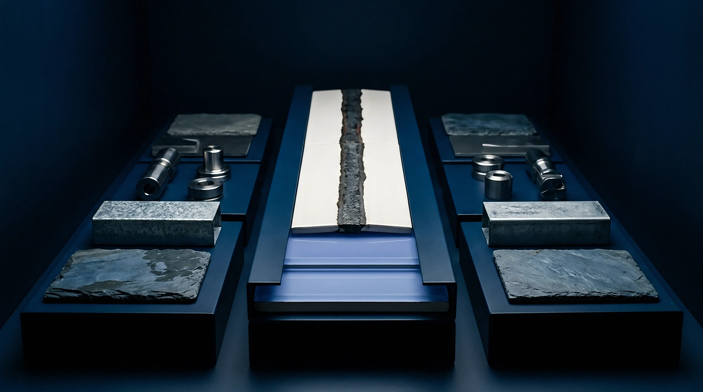
Encapsulation keeps delicate circuit board features from distorting during coarse grinding steps. Cold-mounting acrylic resins cured at room temperature avoid thermal expansion stresses that alter the gold-nickel boundary. Epoxy systems with minimal cure shrinkage maintain sharp edge retention far better than fast-curing acrylics.
Preserving flat, clean edges across the copper, electroless nickel, and immersion gold stack is necessary to measure boundary spike depths accurately under the microscope.
Resin Selection and Vacuum Impregnation Protocols
Hot compression mounting subjects samples to pressures up to thirty megapascals at one hundred eighty degrees Celsius. That level of thermal stress cracking brittle nickel-phosphorus layers is frequently mistaken for actual plating hyper-corrosion. Liquid epoxy systems coupled with vacuum degassing pull air from blind micro-vias and surface features.
Holding a vacuum of sixty kilopascals for five minutes clears trapped air along the PCB surface, providing solid structural support right up to the gold interface.
- Coupon Extraction Cut the target PCB section using a diamond-coated wafering saw operating below five hundred revolutions per minute under continuous liquid coolant flow.
- Fixtures Setup Secure the extracted specimen in plastic support clips, ensuring the cross-sectional face rests perpendicular to the bottom of the mounting mold.
- Resin Dosing Mix low-viscosity epoxy resin and amine hardener at the exact mass ratio specified by the formulation datasheet to prevent incomplete cross-linking.
- Vacuum Evacuation Place the filled molds inside a vacuum chamber, cycling atmospheric pressure twice to draw trapped gas out of surface cavities.
- Curing Hold Retain the mounted sample at ambient temperature for twelve hours to allow full polymerization without exothermic heat generation.

Grinding and Polishing Mechanical Sequence
Coarse silicon carbide paper damages brittle nickel layers below the surface. A step-down sequence through finer grits removes the deformation left by earlier abrasives. Automated polishing tables control downward force to prevent relief polishing, where softer copper and gold wear down faster than hard electroless nickel.
Keeping the abrasion uniform keeps hyper-corrosion spikes sharp and in focus across the sample.
IPC-4552B mandates that cross-sectional micro-section preparations maintain planarity within two degrees to prevent optical depth distortion of hyper-corrosion features.
Polishing cloths with monocrystalline diamond suspension down to one micrometer clear out residual grinding scratches. A final pass using colloidal silica at 0.04 micrometers creates a mirror finish ready for high-magnification optical and electron microscopy. Skipping steps leaves scratch patterns that look like corrosion channels.
While fast manual polishing is sometimes used under time pressure, variations in hand pressure consistently round off edges.

Spike
Microscopic analysis separates minor plating variations from actual hyper-corrosion spikes that destroy solder joint integrity. Scanning electron microscopy at magnifications between five thousand and fifteen thousand times resolves micro-spike shapes clearly. Optical microscopes cannot reliably distinguish true intergranular spikes from shallow surface pitting when feature widths drop below 0.2 micrometers.
Measuring defect depth against overall nickel thickness gives the quantitative ground needed for lot rejection.

Categorizing Corrosion Depth and Defect Geometry
Hyper-corrosion spikes run vertically through the electroless nickel layer, creating fissures that cut down the load-bearing area of solder joints. IPC specifications establish threshold classifications based on how far spikes penetrate relative to nominal nickel thickness. An isolated spike extending less than twenty percent into the layer generally allows normal intermetallic growth during reflow assembly.
Multiple continuous spikes passing thirty percent signal severe bath degradation and call for immediate containment.
Spikes take three main shapes under high-resolution imaging. Type one shows as broad, shallow planar degradation along the nickel boundary. Type two forms narrow, V-shaped notches extending down crystal domain walls.
Type three appears as deep, needle-like channels reaching all the way to the copper substrate, carrying a high risk of complete solder joint separation under mechanical shear stress.

Is Optical Microscopy Adequate for Resolving Hyper-Corrosion Spikes?
Light microscopy at one thousand times magnification offers a quick sanity check for gross plating flaws and overall layer thickness. High-numerical-aperture oil immersion lenses resolve features down to roughly 0.25 micrometers under brightfield illumination. However, hyper-corrosion spikes frequently taper to tips under 0.1 micrometers, making them invisible under standard light reflection optics.
Scanning electron microscopy paired with energy-dispersive X-ray spectroscopy confirms whether a dark feature is an open void or simply a phosphorus-rich boundary phase.
| Evaluation Criterion | Optical Microscopy (1000x) | Scanning Electron Microscopy (5000x+) |
|---|---|---|
| Maximum Spatial Resolution | Approximately 250 nanometers | Better than 3 nanometers |
| Subsurface Spike Detection | Limited to wide, oxidized fissures | Resolves narrow, sub-micron intergranular spikes |
| Compositional Analysis | Not available (visual contrast only) | EDX maps phosphorus, nickel, gold, and copper concentrations |
| Preparation Sensitivity | High sensitivity to surface relief and stains | Requires conductive coating if mount charging occurs |
Solder joint reliability drops sharply once hyper-corrosion density passes five distinct spikes per linear millimeter. Field failures in high-vibration environments show clear cleavage fractures along the phosphorus-rich nickel-tin intermetallic interface containing these spikes. Just where micro-spikes transition from benign bath signatures into active failure sites remains a point of debate among engineers working on high-reliability automotive assemblies.


Audit
Sampling plans dictate how many micro-section samples auditors pull from PCB lots to check ENIG compliance. Pulling a single coupon per panel often misses localized spikes caused by uneven fluid flow in plating tanks. Tank edges routinely see higher current densities and stagnant fluid compared to the center.
Testing multiple coupons across the panel surface provides a clearer picture of plating variation before boards head to assembly.

Sampling Ratios and Quality Assurance Frameworks
Standard quality control calls for three micro-section coupons per plating rack to capture spatial variance inside the immersion gold tank. Pulling panels from the top, middle, and bottom of the flight bar highlights dead zones in bath circulation. Inspection teams perform destructive cross-sectioning on designated quality coupons run alongside production boards.
A lot fails when any single coupon shows Level 3 hyper-corrosion spikes penetrating past thirty percent nickel thickness across three inspected fields of view.
- Coupon Location Standard Collect test coupons from opposing diagonal corners and the center of each production panel array.
- Field Count Standard Examine a minimum of ten independent fields of view per cross-sectioned coupon at 5000x magnification under SEM.
- Data Record Standard Log nickel thickness, gold thickness, phosphorus percentage, and maximum spike depth into statistical process control tracking sheets.
- Rejection Trigger Standard Stop production immediately if three consecutive panels display hyper-corrosion spikes exceeding twenty percent nickel thickness.

IPC-4552B Compliance Requirements
The IPC-4552B specification sets limits for nickel corrosion levels across printed circuit board lots, ranging from Level 0 with no visible corrosion to Level 3 showing continuous, severe corrosion spikes along the nickel interface. Compliance means documenting mean gold thickness using X-ray fluorescence while confirming surface integrity through destructive cross-sectioning. Skipping destructive sectioning leaves hyper-corrosion undetected, as non-destructive X-ray methods read total metal mass without revealing internal voids.
Section 4.3 of IPC-4552B specifies that visual micro-section inspection takes precedence over non-destructive optical tools when adjudicating lot acceptance disputes.
Contracts between buyers and fabricators rely on these IPC standards to establish clear grounds for batch rejection. Receiving inspectors send panel coupons directly to failure analysis labs when X-ray fluorescence shows abnormally high gold thickness. Gold readings above 0.10 micrometers align closely with aggressive nickel dissolution and spike formation.
Standard purchase terms require full lot replacement at the supplier’s expense upon verified laboratory confirmation of Level 3 hyper-corrosion defects.


Exposure
Latent hyper-corrosion defects often stay hidden until components pass through surface mount soldering and thermal testing. Scrapping an unpopulated bare board costs very little compared to losing a fully populated board during final testing. Air-freighting replacement bare boards to assembly lines does nothing to recover lost production time or ruined active components attached to defective ENIG pads.
Working out total financial exposure means factoring in board procurement, lost components, rework labor, and line downtime.
Rework Arithmetic and Containment Calculations
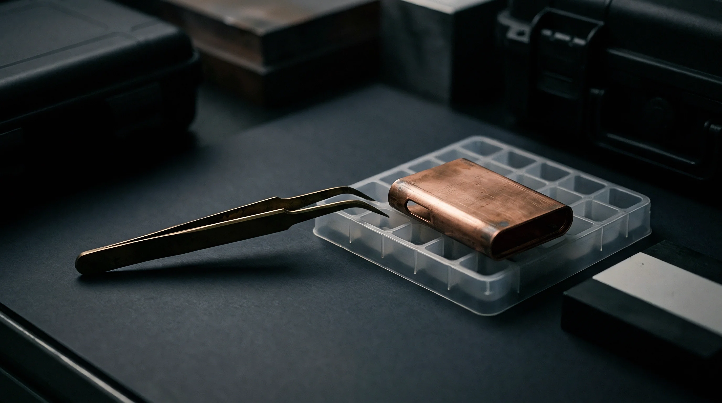
Evaluating risk requires walking through a standard assembly scenario. Take a production run of five thousand populated boards with a bare-board cost of twelve dollars each. Active components on each assembly add ninety-five dollars in material value, while assembly labor and SMT line time run fifteen dollars per unit.
That puts baseline manufacturing cost at one hundred twenty-two dollars per unit, representing a total lot commitment of six hundred ten thousand dollars.
When hyper-corrosion spikes cause solder joint dewetting or low-stress fractures during testing, manual rework is rarely an option. Joints fail at the nickel-phosphorus boundary underneath the intermetallic layer, so touching them up with a soldering iron accomplishes nothing. Scrapping the populated board means losing the full one hundred twenty-two dollars.
Desoldering parts to salvage expensive microprocessors recovers roughly forty percent of active component value while adding eight dollars per unit in technician labor.
| Discovery Phase | Direct Scrapped Material | Rework and Labor Overhead | Net Financial Loss per 5,000 Units |
|---|---|---|---|
| Bare Board Incoming Audit | $60,000 (Bare boards) | $1,200 (Laboratory sectioning fees) | $61,200 |
| Post-SMT Reflow Testing | $535,000 (Boards and components) | $40,000 (Desoldering and salvage effort) | $385,000 (Net after salvage recovery) |
| Field Operation Failure | $535,000 (Boards and components) | $250,000 (Field warranty and logistics) | $785,000 plus liability exposure |
Catching hyper-corrosion spikes at receiving inspection costs sixty-one thousand two hundred dollars including lab fees. Finding the same defect after surface mount assembly raises the net loss to three hundred eighty-five thousand dollars, even assuming decent component recovery. Field returns drive total losses past seven hundred eighty-five thousand dollars once warranty claims and reverse logistics hit.
Running destructive micro-sectioning on incoming coupons easily covers its annual budget by catching a bad plating lot before it ever reaches the SMT line.