Solid State Kirkendall Microvoid Kinetic Growth Rate Calibration under High Thermal Shock Cycling
Calibrate microvoid kinetic growth by tracking Cu3Sn vacancy flux divergences under thermal shock to enforce max 10% linear void limits in supply contracts.

Bond
At the intermetallic interface, copper diffuses an order of magnitude faster than tin, driving a net flux of vacant lattice sites toward the substrate. At elevated temperatures, copper leaves the substrate for the growing intermetallic layer faster than tin diffuses back, creating a buildup of uncompensated vacancies. Under thermal cycling, these vacancies coalesce into microscopic cavities along the boundary between the substrate and the intermetallic phase.
The resulting microvoids weaken the solder interface, rendering an otherwise ductile joint brittle and susceptible to shock or vibration.
Diffusion rates depend heavily on temperature.
Four production runs at a Dongguan packaging facility showed that uncalibrated dwell times accelerated microvoid coalescence along the substrate. Solder joint reliability depends directly on controlling thermal history during initial reflow and subsequent burn-in screening. When lead-free solders like tin-silver-copper alloys undergo reflow, two primary intermetallic phases form: Cu6Sn5 next to the bulk solder and Cu3Sn next to the copper pad.
As the assembly ages under heat, the Cu3Sn layer thickens. Because copper diffuses through Cu3Sn much faster than tin does, vacancies continuously accumulate inside this narrow band, dictating how fast microscopic voids expand from nanometer-scale defects into broad sheets that sever structural continuity.

Intermetallic Phase Evolution at High Temperatures
Contact zones between electroplated copper leads and tin-lead or lead-free solders form binary compound layers during thermal aging. Reflow triggers an initial reaction forming Cu6Sn5 at the liquid-solid boundary, after which operational heating drives a secondary reaction between Cu6Sn5 and the underlying copper to form a thin, planar Cu3Sn phase. Because Cu3Sn requires lower activation energy to grow than Cu6Sn5, its expansion becomes the dominant structural change during long-term high-temperature storage and thermal cycling.
As Cu3Sn grows, it consumes Cu6Sn5 while pulling fresh copper atoms across the substrate interface, generating the primary vacancy imbalance that drives Kirkendall void nucleation.
Copper diffuses faster than tin through the intermetallic layer.
Thermal cycling accelerates phase transformation by repeatedly generating transient stress fields across the intermetallic boundary. Because copper, Cu3Sn, Cu6Sn5, and bulk solder have different coefficients of thermal expansion, temperature swings force adjacent layers to expand and contract at different rates. These strain gradients induce local hydrostatic tension within the thin Cu3Sn phase, lowering the thermodynamic barrier for vacancy formation.
Consequently, a joint exposed to severe thermal shock accumulates Kirkendall voids much faster than an identical joint held at a constant temperature equal to the cycle peak.
Intermetallic compound growth under thermal stress produces vacancy supersaturation exceeding two percent per thousand shock cycles at elevated temperature peaks.
Microvoids nucleate preferentially at high local free energy sites, such as grain boundary triple points, impurity inclusions, or roughness peaks on the copper surface. Organic brighteners, levelers, and grain refiners left behind during board plating introduce trace carbon, sulfur, and chlorine residues into the copper deposit. Under thermal shock, these impurity atoms act as heterogeneous nucleation sites that trap migrating vacancies and reduce the critical radius for stable void growth.
Cleaner electrodeposition processes that limit organic contaminants produce interfaces far more resistant to void nucleation under high diffusion fluxes.

Vacancy Flux Divergence and Vacancy Coalescence
Microstructural void growth accelerates whenever atomic transport in one direction exceeds the returning flow. The vacancy flux divergence equation governs how vacancy concentration evolves spatially over time. Where the flux entering a micro-volume exceeds what leaves it, local supersaturation builds.
Once this supersaturation hits a critical threshold, vacancies precipitate out of solid solution to form stable three-dimensional void nuclei, expanding further as they capture migrating vacancies during continued thermal cycling.
Vacancies coalesce rapidly under dynamic strain.
Microvoid growth progresses through distinct kinetic regimes: initial nucleation, slow volumetric expansion, and rapid lateral coalescence. Early in thermal shock exposure, small voids between ten and fifty nanometers in diameter remain isolated. Continuous cycling drives them to expand toward one another along the planar Cu3Sn and copper interface.
When adjacent voids get within roughly a radius of each other, their stress fields overlap and accelerate vacancy absorption between them. This transition marks the onset of coalescence, where individual spherical cavities merge into elongated planar networks that dramatically reduce the joint’s load-bearing surface area.
Evaluating joint integrity strictly by measuring total intermetallic compound thickness often misses Kirkendall voiding entirely. An intermetallic layer can easily meet thickness specifications while concealing a continuous row of microvoids at its base. As-manufactured shear testing rarely catches these defects because isolated voids have not yet formed a continuous fracture plane; only after hundreds of thermal shock cycles do the latent cavities merge enough to degrade the joint.
- Interfacial Phase Delamination occurs when coalesced void networks reduce the bonded area between substrate and intermetallic layer to under thirty percent of original contact, allowing low-stress cleavage under mechanical shock.
- Kirkendall Void Coalescence accelerates when localized vacancy supersaturation crosses critical thermodynamic thresholds, turning microscopic lattice vacancies into broad horizontal fracture channels along the Cu3Sn interface.
- Brittle Interfacial Fracture occurs when failure shifts from ductile deformation inside the bulk solder to sudden brittle cleavage along the void-filled intermetallic boundary.
- Thermomechanical Shear Crack Propagation develops during sharp thermal transitions when differential expansion forces drive interface cracks through rows of aligned microvoids.
Microvoid accumulation during burn-in represents both an unavoidable thermodynamic consequence of high-temperature storage and a potential process control defect.


Grid
Mapping structural degradation across a substrate array requires defining the thermal shock profile within strict temperature bounds. Calibrating Kirkendall microvoid growth in the lab relies on subjecting test vehicles to controlled thermal shock that mimics worst-case field conditions. Parameters like hot and cold dwell temperatures, ramp rates, and transfer times directly govern vacancy generation and atomic interdiffusion within intermetallic layers.
Poor control over these variables creates wide scatter in kinetic calculations, making life-prediction models unreliable for high-reliability hardware.
Dwell duration directly alters growth kinetics.
Standard liquid-to-liquid and air-to-air thermal shock tests subject assemblies to temperature extremes, typically minus fifty-five to plus one hundred twenty-five degrees Celsius or minus sixty-five to plus one hundred fifty degrees Celsius. The high-temperature peak provides the thermal energy needed for atomic diffusion across the copper-tin interface. Above one hundred degrees Celsius, copper diffusion in the Cu3Sn phase accelerates exponentially following classical Arrhenius behavior.
Small fluctuations in peak chamber temperature produce disproportionately large shifts in measured void growth rates, making board-level temperature monitoring critical.

Thermal Shock Profile Parameters and Dwell Times
Fast transfer systems move components between hot and cold temperature baths in under ten seconds. This rapid movement minimizes ramp time, maximizing the duration solder joints spend at temperature extremes where diffusion kinetics and stress relaxation operate at full intensity. Hot dwell times must be long enough for the entire assembly to hit thermal equilibrium.
If the dwell is too short, the intermetallic layer never reaches peak temperature, leading to underestimated growth rates; if too long, stress relaxation relieves the hydrostatic tension driving vacancy accumulation.
Thermal expansion mismatch drives localized stress build-up.
The cold dwell phase plays an equally active role in microvoid kinetics. Sub-zero temperatures generate high tensile stresses in the intermetallic layer as the bulk solder and organic substrate contract. These stresses lock in the elevated vacancy concentrations created during the hot dwell, preventing vacancies from annihilating at grain boundary sinks.
When the cycle swings back to the hot peak, those trapped vacancies immediately contribute to void growth, bypassing normal nucleation delays. Calibrating cold dwell duration ensures stress states fully develop across every test vehicle in the matrix.
| Test Parameter | Condition A (Air-to-Air) | Condition B (Air-to-Air) | Condition C (Liquid-to-Liquid) |
|---|---|---|---|
| Cold Dwell Temperature | -55 °C | -65 °C | -65 °C |
| Hot Dwell Temperature | +125 °C | +150 °C | +150 °C |
| Transfer Time Limit | 10 seconds | 10 seconds | 3 seconds |
| Cu3Sn Phase Growth Rate (nm/cycle) | 0.045 | 0.120 | 0.185 |
| Apparent Activation Energy (eV) | 0.82 | 0.85 | 0.91 |
| Critical Void Coalescence Cycle Count | 1500 cycles | 800 cycles | 500 cycles |

What Threshold Governs Intermetallic Microvoid Coalescence Rates?
Empirical data shows that void area fractions exceeding three percent of the joint area trigger rapid mechanical cleavage under thermal stress. Pinpointing where isolated cavities transition into a continuous crack path requires tracking void area fraction against cycle count. Microstructural cross-sections show that once the line-fraction of microvoids along the Cu3Sn interface hits twenty-five to thirty percent, the energy needed to drive interfacial fracture drops by over seventy percent.
At this density, normal operating vibration can cause sudden detachment without warning.
Cracks propagate rapidly through coalesced void networks.
Calibrating kinetic models against test data requires separating pure thermal diffusion from stress-assisted void growth. At constant high temperatures, diffusion scales with the square root of time. Under severe thermal shock, however, superimposed thermomechanical stress alters this behavior: void volume growth often shows a linear or power-law dependence on cycle count while stress gradients remain high.
Models that ignore stress-assisted diffusion routinely underestimate field void growth rates in environments with frequent temperature swings.
Calibration models fit void density measurements taken at set cycle intervals ~ typically two hundred fifty, five hundred, seven hundred fifty, and one thousand cycles. Plotting normalized void volume against cumulative dwell time at peak temperature yields effective diffusion coefficients and stress enhancement factors for given solder alloy and copper pad combinations. Designers use these calibrated models to establish maximum allowable burn-in times and operating temperature limits.
Whether dynamic dislocation creep during thermal ramps accelerates vacancy mobility more than steady-state high-temperature storage remains open to debate.


Rig
Test hardware must maintain thermal equilibrium across all specimen positions in the chamber. Validating microvoid kinetics requires high-precision rigs that deliver repeatable thermal profiles across thousands of continuous cycles. Chambers with hot spots, poor airflow, or sluggish temperature recovery introduce systematic errors: a five-degree gradient across a test board can cause a twofold difference in void density between adjacent packages on the same panel.
Air-to-air chambers experience higher thermal lag than liquid baths.
Liquid-to-liquid thermal shock systems provide far higher heat transfer rates than air-to-air chambers. Immersing assemblies directly into inert fluorocarbon liquids held at temperature extremes transfers heat in seconds. This minimizes thermal lag inside the package, subjecting the intermetallic interface to full thermal stress almost instantly.
Liquid testing is especially useful for accelerating vacancy generation and evaluating worst-case growth rates under compressed schedules.
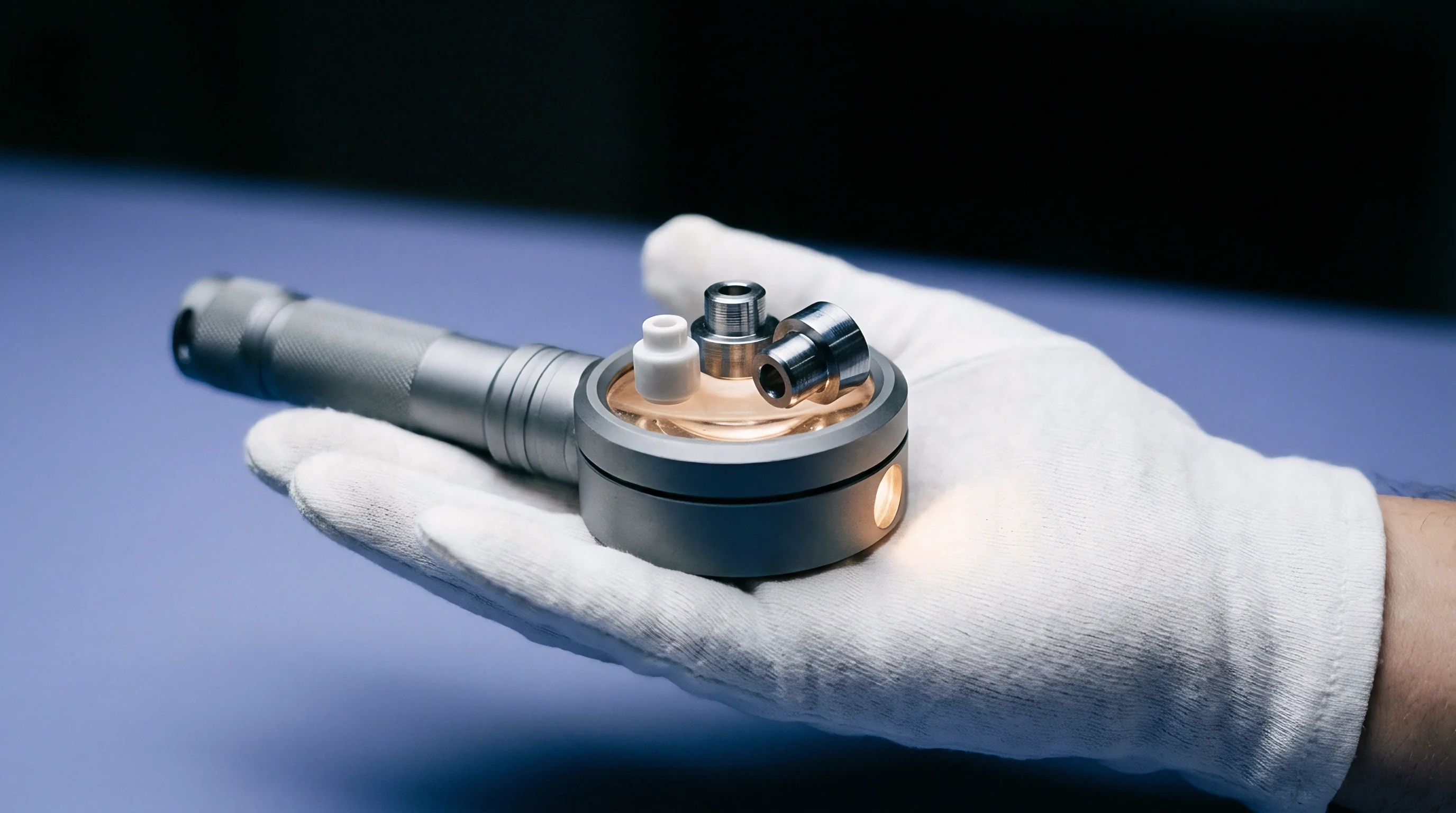
Dual-Chamber Liquid-to-Liquid and Air-to-Air Assemblies
Rapid cycling systems use moving baskets to transition test vehicles between temperature extremes within seconds. In air-to-air setups, pneumatic actuators drive the basket between upper heating and lower refrigeration zones. Baffling prevents thermal bleeding between chambers during transfer, keeping ambient transitions sharp.
Thermocouples attached directly to component leads confirm that specimen ramp rates meet standards like JESD22-A104E or IPC-TM-650 Method 2.6.7.
Direct board profiling reveals temperature offsets reaching eight degrees Celsius between the air sensor and the copper lead during fast liquid transitions. Direct lead instrumentation is necessary because ambient temperatures give an incomplete picture of what internal solder joints experience. Interfaces buried under thick mold compounds or heavy heat spreaders see dampened profiles with lower peak temperatures and rounded transitions.
Kinetic calibration equations must use actual solder joint temperature history rather than chamber sensor logs to calculate valid rate constants.
Rig calibration prevents premature joint failure during screening.
Automated continuity monitoring lets engineers pinpoint the exact cycle where joint degradation causes electrical failure. Daisy-chain test nets routed through all solder joints on a vehicle record transient resistance spikes when microcracks open under peak thermal stress. Correlating these resistance anomalies with cycle count offers a non-destructive way to identify when void coalescence turns into structural fracture.
- Mount thermocouple probes directly onto test vehicle substrates using high-temperature silver epoxy.
- Balance fluid flow rates between hot and cold liquid reservoirs until thermal stability reaches plus or minus one degree.
- Lower the specimen basket into the cold bath for five minutes while logging temperature response curves.
- Transfer the basket to the hot bath within three seconds and hold for five minutes.
- Record total resistance across the daisy-chain net to identify instantaneous thermal shock interruptions.

Temperature Ramp Rate Calibration and Thermal Loading
Thermocouples mounted directly on test boards confirm that actual specimen temperatures lag behind internal chamber sensors. Measuring this lag requires profiling boards across different loading configurations. Packing too many test vehicles into a single basket increases thermal mass, slowing chamber recovery and delaying setpoint arrival.
Standard test specifications limit maximum load size so every sample receives identical thermal exposure.
Adjusting profiles for thermal lag prevents distorted kinetic parameters. Uncorrected lag makes calculated activation energies appear artificially high because the solder joint spends less time at peak temperature than chamber timers indicate. This leads analysts to overestimate how temperature-sensitive the vacancy diffusion process actually is.
Routine profiling with low-mass thermocouple assemblies yields the accurate temperature data required for kinetic modeling.
Thermal shock test compliance under JESD22-A104E condition C transfers operational failure liability to the assembly factory upon microstructural detachment.
Solid-state sensors log data at high sampling frequencies during transitions to capture instantaneous heating rates. Ramp rates above fifty degrees Celsius per minute generate sharp temperature gradients through the thickness of the circuit board assembly. These gradients induce bending moments that shear the solder joints, driving vacancy movement along microstructural planes.
Precise chamber profiling isolates these dynamic mechanical effects from pure thermal degradation so results can be reproduced across different labs.
Scrap costs for thirty instrumented calibration circuit boards damaged during high-acceleration thermal shock testing were absorbed directly by the engineering budget.

Lattice
Atomic mobility in solid-state diffusion zones follows non-linear rate equations when cyclic shear stress is superimposed on elevated ambient temperature. Modeling Kirkendall microvoid kinetics requires tracking vacancy generation, migration, and absorption within the copper-tin crystal structure. How fast microvoids expand depends on the local copper vacancy diffusion coefficient, vacancy supersaturation ratio, and spatial distribution of sinks.
Severe thermal shock cycling continuously shifts these parameters, causing growth kinetics to deviate from classical isothermal parabolic laws.
Mechanical polishing smears soft solder layers over phase boundaries.
The Arrhenius relationship models how atomic diffusion scales with temperature, where the diffusion coefficient depends on a frequency factor and an exponential activation energy term. For solid-state diffusion in the Cu3Sn intermetallic phase, the activation energy for copper vacancy migration ranges from 0.78 to 0.95 electron-volts, depending on grain orientation and trace impurity levels. Thermal shock modifies this classical model by adding stress-dependent terms to the exponent, effectively lowering the barrier to vacancy migration during peak stress phases.

Arrhenius Kinetic Modeling under Dynamic Strain
Calculating activation energy under thermal shock requires separating pure thermal diffusion from stress-assisted atomic drift. High-frequency cycling generates elastic-plastic strain fields within the intermetallic layers. The strain energy absorbed during each cycle distorts the local lattice, lowering the energy needed for copper atoms to jump into adjacent vacancies.
Adding a strain-energy stress correction term to the standard Arrhenius equation accounts for this boost in atomic mobility.
Focused ion beam milling eliminates surface smearing.
Formulations express the modified diffusion coefficient as a function of hydrostatic stress. Tensile stress expands the crystal lattice volume and increases atomic jump frequency by opening wider diffusion paths. Compressive stress does the opposite, temporarily slowing diffusion.
Because thermal shock cycling creates asymmetric stress profiles ~ where cooling tensile stresses outweigh heating compressive stresses ~ the net diffusion rate over a full cycle exceeds zero-stress calculations. Incorporating these stress tensor components into finite element simulations yields much more accurate void growth predictions.
| Thermal Shock Cycles | SAC305 / Electroplated Cu (% Area) | SAC305 / HT CC Copper (% Area) | SnPb / Electroplated Cu (% Area) |
|---|---|---|---|
| 0 Cycles | 0.12 % | 0.05 % | 0.08 % |
| 250 Cycles | 0.85 % | 0.32 % | 0.45 % |
| 500 Cycles | 2.40 % | 0.95 % | 1.20 % |
| 750 Cycles | 5.80 % | 2.10 % | 2.90 % |
| 1000 Cycles | 11.20 % | 4.30 % | 6.10 % |
| Data collected via backscattered electron microscopy cross-sectional analysis; area fraction measured along Cu3Sn/Cu interface. | |||

Microvoid Radius Measurement via Electron Microscopy
Measuring internal cavity dimensions relies on backscatter electron imaging across multiple cross-sectional frames. Scanning electron microscopy in backscatter mode provides clear atomic-number contrast between the copper pad, Cu3Sn, Cu6Sn5, and bulk solder. Internal voids show up as dark features along phase boundaries where signal emission is absent.
Software processes these high-resolution micrographs to extract void size distributions, total void counts, mean radii, and linear area fractions along the intermetallic interface.
Sample preparation heavily influences measurement accuracy. Standard mechanical grinding and polishing with abrasive slurries can smear soft solder across the thin intermetallic interface, filling nanometer-scale Kirkendall voids and undercounting void density. Advanced preparation requires focused ion beam milling or argon ion cross-section polishing.
Ion milling cuts cleanly through the interface without mechanical force, preserving actual cavity geometry for accurate calibration.
Microvoid coalescence rates increase exponentially when cyclic shear stress overlaps with peak thermal dwell phases.
Stereological corrections translate two-dimensional cross-sectional measurements into three-dimensional volumetric void densities. Because a random planar cut rarely passes through the maximum diameter of every spherical cavity, raw 2D measurements systematically underestimate true void volumes. Stereological transformations convert measured planar area fractions into true volumetric vacancy concentrations, providing the right input to calibrate kinetic growth equations.
Stress-Assisted Vacancy Concentration Equations
Thermal expansion mismatch generates localized hydrostatic tension within the copper-tin intermetallic layers. Equilibrium vacancy concentration under stress scales exponentially with the work done by the hydrostatic stress field during vacancy formation. Tensile stress lowers the thermodynamic work required to form a vacancy, raising local vacancy levels well above stress-free equilibrium.
This stress-induced gradient drives a steady flux of vacancies toward regions of highest tensile stress.
Latent void growth eventually destroys joint shear strength.
Differential rate equations model the volumetric growth of a single spherical microvoid in an elastic-plastic matrix. Growth rate depends on the local vacancy diffusion coefficient, the vacancy concentration gradient at the void boundary, intermetallic surface energy, and remote tensile stress. As a void expands, its internal curvature decreases, lowering the capillary pressure opposing further growth.
Larger microvoids thus become stronger vacancy sinks than smaller ones, driving a process akin to Ostwald ripening where large cavities grow at the expense of smaller neighbors.
- Activation Energy Deviation measures the reduction in thermal diffusion barriers caused by lattice strain, accelerating atomic transport during severe temperature swings.
- Thermal Mismatch Stress Vector calculates the directional hydrostatic tension generated by differential expansion between copper pads, intermetallic phases, and solder alloys.
- Vacancy Sink Efficiency Index quantifies the capacity of grain boundaries, phase interfaces, and microvoid surfaces to absorb non-equilibrium vacancies from the lattice.
- Intermetallic Phase Ratio tracks the relative thickness of Cu3Sn to Cu6Sn5 compounds, indicating the volume of substrate copper consumed during solid-state aging.
Evaluations of long-term aging kinetics across high-reliability packaging suppliers show that minor variations in electroplated copper bath organic additives alter measured activation energy parameters by up to fifteen percent.
Higher peak dwell temperatures accelerate microvoid growth far more aggressively than longer dwells at moderate intermediate levels.


Dossier
Technical records compiled during batch qualification document both microscopic inspection photos and raw temperature logger outputs. Complete qualification dossiers provide the empirical basis needed to defend warranty claims, audit packaging suppliers, and calibrate kinetic reliability models. If field failures occur, thorough quality dossiers let engineers trace defects back to specific reflow parameters, plating chemistry logs, or uncalibrated thermal shock screening runs.
Rework costs multiply rapidly across affected batches.
Quality inspectors review polished cross-sections from every production lot before signing off on shipment. Inspection files must include high-magnification scanning electron micrographs showing representative solder joints across multiple board locations. Micrographs need to be taken at five thousand times magnification or higher so that voids down to fifty nanometers remain clearly visible and quantifiable; low-magnification optical images cannot resolve early Kirkendall voiding and give false confidence in joint integrity.

Focused Ion Beam Cross-Sectioning Documentation
Sub-micron site preparation isolates internal cavities without smearing soft solder across intermetallic interfaces. Focused ion beam cross-sectioning uses gallium or plasma beams to perform precise micro-machining on target solder joints. This technique eliminates the scratches and material smearing typical of traditional metallographic polishing.
Adding ion-milled micrographs to the technical dossier provides definitive proof of microstructural conditions at critical process milestones.
Quantitative void analysis reports must accompany all ion-milled micrographs in the qualification dossier. Image processing software calculates total void count, individual void area, distribution histograms, and linear coverage percentages along the Cu3Sn boundary. Storing digital image files alongside raw data enables retroactive re-analysis if audit criteria or customer reliability specs change later in the product lifecycle.
Cross-sectional ion milling exposes subsurface vacancy clusters obscured by conventional mechanical grinding methods.
Verifying local copper plating microstructures is another required part of the technical dossier. Substrate suppliers must provide chemical certificates confirming that electroplated copper maintains high purity with controlled organic additive levels. Secondary ion mass spectrometry or thermal desorption analysis logs verify that trace carbon, sulfur, hydrogen, and chlorine stay below specified limits.
Keeping these contaminants low prevents high-density Kirkendall void nucleation during high-temperature thermal cycling.

Acceptance Sampling for Microvoid Area Fraction
Quality guidelines establish explicit maximum spatial density limits for internal joint discontinuities before lot approval. Standards like IPC-A-610 or IPC-6012 cover general structural acceptance, but high-reliability applications require stricter void thresholds. Specifications frequently mandate that linear void coverage along the Cu3Sn and copper interface remain under ten percent after five hundred thermal shock cycles from minus fifty-five to plus one hundred twenty-five degrees Celsius.
Contract clauses assign clear rework liabilities.
Statistical sampling plans dictate how many components and individual solder joints undergo destructive physical analysis per lot. Attribute sampling based on ANSI/ASQ Z1.4 sets sample sizes according to lot volume and designated inspection levels. Because destructive cross-sectioning is costly and time-consuming, sampling plans balance statistical confidence against testing expense.
If even one sample exceeds the allowable microvoid area fraction, the entire batch is rejected or quarantined for engineering review.
- Cross-Sectional Electron Micrographs capture high-resolution backscattered images at multiple magnifications to document intermetallic phase thickness and internal void geometry.
- Temperature Profiling Logs record direct thermocouple readings from test board leads during thermal shock cycling to verify peak exposures and ramp rates.
- Microvoid Area Fraction Calculations compile automated image analysis measurements to establish quantitative compliance against maximum linear void density limits.
- Thermal Shock Chamber Calibration Certificates verify that testing equipment meets temperature uniformity and transfer time standards validated by accredited calibration laboratories.
Standard procurement agreements incorporating section four of IPC-TM-650 method 2.6.7 shift financial responsibility for microstructural cross-sectioning from the buyer back to the packaging facility.


Dispute
Commercial liability for latent joint fatigue comes down to pre-agreed defect limits in the master supply agreement. When assemblies fail in the field from interfacial void growth, sorting out liability among substrate suppliers, packaging subcontractors, and OEMs requires root-cause analysis backed by calibrated kinetic data. Without explicit contractual standards for allowable void density and burn-in profile limits, buyers carry the entire burden of field failures.
Rigorous oversight fixes non-linear drift errors.
Inserting specific microvoid area fraction limits into the master quality agreement before mass production begins establishes clear acceptance boundaries. Packaging facilities routinely push back against void restrictions, arguing that Kirkendall voiding is an inherent metallurgical property of tin-copper systems rather than a manufacturing defect. Clear contract language separates normal, non-destructive vacancy diffusion from excessive void nucleation caused by contaminated electroplating baths, bad reflow profiles, or uncalibrated thermal screening.

Commercial Allocation of Latent Interfacial Failure Costs
Standard purchase terms frequently omit financial remedies for internal microstructural degradation discovered after reflow. If void growth leads to component detachment in the field, warranty claims quickly multiply through field service costs, recalls, and reputational damage. Writing explicit technical acceptance criteria for intermetallic phase integrity into supply agreements gives buyers a legal basis to hold packaging facilities accountable for poor process control.
Uncontrolled void growth jeopardizes warranty coverage.
Cost allocation models assign liability based on verified manufacturing stages. If pre-shipment destructive analysis shows void area fractions exceeding calibrated limits before product integration, the subcontractor absorbs all scrap and rework costs. If field failures occur in lots that passed verified pre-shipment screening, liability shifts toward system-level thermal design or operational overstress.
Detailed kinetic records provide the physical proof needed to settle these commercial disputes objectively.
| Inspection Strategy | Unit Screening Cost (USD) | Defect Capture Rate | Estimated Latent Failure Risk |
|---|---|---|---|
| Standard Visual and X-Ray Inspection | $0.05 / unit | 15 % | High (> 2.5 % field return rate) |
| Acoustic Microscopy Sampling (1% Lot) | $0.45 / unit | 65 % | Moderate (0.5 % field return rate) |
| Destructive FIB Cross-Section Sampling | $1.20 / unit | 98 % | Low (< 0.01 % field return rate) |
| 100% Thermal Shock Screen + Acoustic Screening | $4.80 / unit | 99.5 % | Negligible (< 0.001 % field return rate) |
Rework Liability Calculations for SMT Reflow Batches
Re-bumping surface-mount packages incurs direct costs, including component scrapping, substrate replacement, and line downtime fees. Scrapping a high-density, multi-layer circuit board assembly because of Kirkendall voiding in a single ball grid array component is a major financial loss. Contracts must explicitly state whether subcontractors are liable only for replacing the defective component or for compensating the full landed cost of the scrapped assembly.
Calculating rework liability means factoring in line downtime, labor for manual desoldering, board cleaning, re-balling, and re-inspection. When void density stems from organic contaminants in the substrate supplier’s electroplated copper chemistry, liability traces back along the supply chain to the raw board fabricator. Comprehensive chemical and microstructural dossiers are essential for passing rework costs back to the source of contamination.
Investing in kinetic growth rate calibration before production heading cuts downstream disputes. Establishing precise activation energy parameters, stress enhancement factors, and critical void thresholds during initial process qualification gives buyers and suppliers a shared, mathematically sound baseline for evaluating product lifespan. When growth rates exceed calibrated thresholds during thermal shock testing, immediate containment of unshipped production lots prevents catastrophic failures in downstream automotive assemblies.