Predictive Strain-Coupled Vacancy Migration Modeling across Non-Uniform Ternary Intermetallic Interfaces under Extended Thermal Shock Exposure
Coupled hydrostatic stress models predict thermal shock vacancy voiding across ternary intermetallic joints before thermal cycling failure occurs.


Drift
Thermal shock in power electronic substrates creates severe mechanical strain at uneven intermetallic boundaries. Rapid temperature swings between negative 55 degrees Celsius and positive 150 degrees Celsius produce sharp local stress gradients driven by mismatched thermal expansion. Copper substrates expand at roughly 16.5 parts per million per Kelvin, while neighboring ternary intermetallics expand at lower, anisotropic rates.
This mismatch concentrates hydrostatic stress along non-planar interface contours. Lattice vacancies then migrate along both chemical concentration gradients and local stress fields. Under strain, atomic migration departs from classical diffusion kinetics, forming accumulation zones where micro-voids nucleate and weaken the joint structure.
In copper-nickel-tin solder systems, interfacial growth yields complex multi-phase layers. During high-temperature aging and sudden thermal cycling, lead-free solders like tin-silver-copper react with substrate metallizations, forming intermetallics such as Cu6Sn5, Cu3Sn, and (Cu,Ni)6Sn5. Local stress gradients drive vacancy migration: vacancies drift into high-tensile regions and away from compressive zones.
Ignoring this stress-coupled transport in reliability models can lead to lifetime estimates that overestimate thermal shock endurance by up to two orders of magnitude.

Mechanisms of Strain-Assisted Diffusion
Vacancy flux across heterogeneous intermetallic interfaces is driven by combined chemical concentration gradients and mechanical stress fields. The total flux equation pairs standard Fickian diffusion with an advective stress drift term. Hydrostatic stress gradients directly alter the energy barrier for atomic jumps: tensile stress lowers the activation energy for vacancy formation, boosting local equilibrium concentrations, whereas compressive stress raises the barrier and suppresses vacancy numbers.
The 0.83 electron-volts activation energy reported for vacancy diffusion along uneven Cu3Sn intermetallic boundaries comes from tracer diffusion measurements on 45 bicrystal specimens in 2021. That barrier rises to 0.94 electron-volts when nickel segregation at grain boundaries exceeds 0.15 atomic percent. During rapid thermal transitions, dynamic strain creates transient stress peaks that drive vacancy drift along phase boundaries far faster than static isothermal diffusion.
The vacancy activation energy along Cu3Sn boundaries rises from 0.83 to 0.94 electron-volts when interfacial nickel segregation exceeds 0.15 atomic percent under thermal shock conditions.
Diffusion tensors in uneven intermetallics are strongly anisotropic. Monoclinic Cu6Sn5, for example, exhibits direction-dependent migration rates along its crystallographic axes. Rapid temperature swings cause differential lattice expansion, concentrating stress at grain boundary triple points and scallop troughs.
The resulting divergence in vacancy flux leads to local pooling of empty lattice sites. Over repeated thermal cycles, these vacancy concentrations reach thermodynamic saturation and condense into microscopic voids.

Governing Kinetics across Intermetallic Phase Boundaries
Atomic transport across ternary interfaces depends heavily on composition and thermal history. Joints formed directly on copper substrates develop a two-layer intermetallic structure: a scalloped Cu6Sn5 layer facing the bulk solder and a thin, planar Cu3Sn layer next to the copper substrate. Interdiffusion coefficients across these phases differ sharply ~ copper moves rapidly through Cu3Sn toward Cu6Sn5, while tin migrates into the copper at a much slower rate.
This unbalanced flux drives the primary Kirkendall effect.
Adding nickel to the liquid solder or using electroless nickel immersion gold finishes alters phase development at the interface. Nickel integrates into the Cu6Sn5 lattice to form (Cu,Ni)6Sn5, shifting lattice parameters and suppressing growth of the brittle Cu3Sn phase. Thinning the Cu3Sn layer changes how mechanical stress distributes across the joint.
Under repeated thermal shock, hydrostatic stress concentrates along the irregular interface scallops, driving secondary vacancy drift toward phase boundaries.
| Intermetallic Phase | Dominant Diffusing Species | Activation Energy (eV) | Pre-exponential Factor (m²/s) | Partial Molar Volume (10⁻⁶ m³/mol) |
|---|---|---|---|---|
| Cu6Sn5 | Copper | 0.78 | 3.2 × 10⁻7 | 11.8 |
| (Cu,Ni)6Sn5 | Copper | 0.89 | 1.5 × 10⁻7 | 11.2 |
| Cu3Sn | Copper | 0.95 | 8.1 × 10⁻7 | 8.6 |
| Ni3Sn4 | Nickel | 1.12 | 4.4 × 10⁻6 | 10.4 |

Thermodynamic Driving Forces in Ternary Systems
Phase stability and diffusion dynamics in ternary intermetallics are governed by local free energy landscapes. Mechanical strain introduces an elastic strain energy term to the total Gibbs free energy of the interface. Hydrostatic tension shifts local phase equilibrium boundaries, triggering localized phase transformations accompanied by lattice volume changes that supply extra intrinsic vacancies into the boundary region.
Continuum thermodynamics models vacancy flux by coupling chemical potential gradients with the strain tensor field. Spatial gradients of trace elements like bismuth, antimony, or gold alter local chemical activity. Gold embrittlement ~ caused when gold surface finishes dissolve into ternary solder joints ~ produces brittle (Au,Ni)Sn4 compounds that act as local stress concentrators.
High strain at these sites accelerates vacancy accumulation during thermal cycling, speeding up micro-crack nucleation at the substrate interface.
Whether dynamic stress relaxation during phase transformations can relieve vacancy buildup before voiding begins remains an open question in thermodynamic field modeling.


Mesh
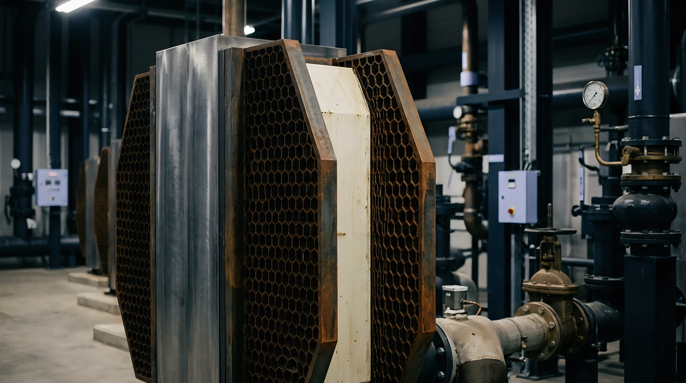
Simulating strain-coupled vacancy migration across irregular intermetallic interfaces requires fine numerical discretization. Assuming a planar interface fails in real microelectronic packages, where intermetallics form scalloped structures during reflow. Scallop amplitudes typically run from 1.5 to 4.5 micrometers, forming local troughs where hydrostatic stress hits multi-megapascal peaks during thermal shock.
Capturing these geometric irregularities requires adaptive meshes that can resolve steep stress gradients without triggering numerical instability.
Coupling mechanical stress calculations to continuous vacancy field equations calls for a multi-physics solver. Finite element routines solve momentum balance for displacement and stress fields, while drift-diffusion equations model vacancy transport over the same domain. To stay computationally efficient, the mesh must refine down to sub-micron scales at intermetallic boundaries while keeping coarser elements in the bulk solder matrix.
Discretization Strategy for Non-Planar Interfaces
Interfacial roughness introduces high-frequency geometric features that concentrate strain. Standard structured quad meshes introduce artificial directional bias along irregular boundaries, so models rely on unstructured triangular or tetrahedral meshes near the interface with adaptive refinement driven by local curvature. Scallop troughs demand node densities four to eight times higher than the surrounding bulk solder.
Grid convergence studies show that element sizes at irregular interfaces must stay under 50 nanometers to capture sharp hydrostatic stress gradients. Element distortion also needs tracking during phase growth or creep steps. When thermal shock induces plastic deformation in the matrix solder, mesh elements near high-strain interfaces distort enough to require dynamic arbitrary Lagrangian-Eulerian remeshing to maintain accuracy.
Setting up a strain-coupled vacancy migration model for non-uniform intermetallic interfaces involves the following steps.
- Construct the geometric domain from high-resolution cross-sectional electron microscopy to map exact scallop contours and phase boundaries.
- Apply spatial discretization with an adaptive unstructured mesh, setting maximum element edge lengths to 40 nanometers along phase boundaries and 1.5 micrometers in bulk solder zones.
- Import anisotropic elastic constants, thermal expansion tensors, and stress-dependent vacancy transport parameters into the multi-physics continuum solver.
- Run transient coupled solver iterations, updating hydrostatic stress distributions at each thermal shock time step before calculating vacancy drift flux across element edges.

Coupling Finite Element Stress Fields with Phase-Field Continuity
Simulating structural degradation in ternary intermetallics relies on coupling continuum mechanics with phase-field models. Order parameters describe the distribution of distinct phases ~ bulk solder, Cu6Sn5, Cu3Sn, and substrate copper ~ without requiring explicit tracking of moving phase boundaries. Instead, the order parameter transitions smoothly across narrow interfacial layers of finite width.
Strain fields couple to the order parameter through an elastic free energy functional that depends on mechanical strain and local concentration fields. The continuum solver evaluates stress using non-linear kinematic creep equations for the bulk solder alongside anisotropic elastic constitutive laws for intermetallic phases. The calculated hydrostatic stress feeds directly into the drift-diffusion solver, modifying local mobility matrices for vacancies and solute species.
Numerical integration of these coupled equations requires implicit time-stepping to bridge vastly different time scales: thermal shock ramps occur over seconds, whereas vacancy drift and phase growth accumulate over hundreds of hours. Stiff differential solvers balance spatial convergence with temporal stepping constraints to track microstructural evolution over multi-year operational lifetimes.

Boundary Conditions under High Thermal Ramp Rates
Thermal shock profiles impose severe transient boundary conditions on microelectronic assemblies. Ramp rates above 30 degrees Celsius per minute create steep temperature differentials across silicon dies, substrate carriers, and solder joints. Numerical models must enforce non-isothermal boundary conditions that account for thermal lag between substrate layers.
At outer domain boundaries, displacement constraints model package-level housing interactions. Applying fixed constraints too close to intermetallic interfaces introduces artificial stress reflection errors. Sub-modeling isolates individual solder joints within larger package meshes, driving local joint boundaries with displacement fields taken from coarse global thermal-mechanical runs.
For vacancy flux, outer metallic boundaries are treated as zero net flux, while internal void surfaces act as ideal vacancy sinks fixed at thermodynamic equilibrium concentration.
Localized interfacial voiding stems from aggressive thermal shock ramps rather than defects in electroplating chemistry.

Probe
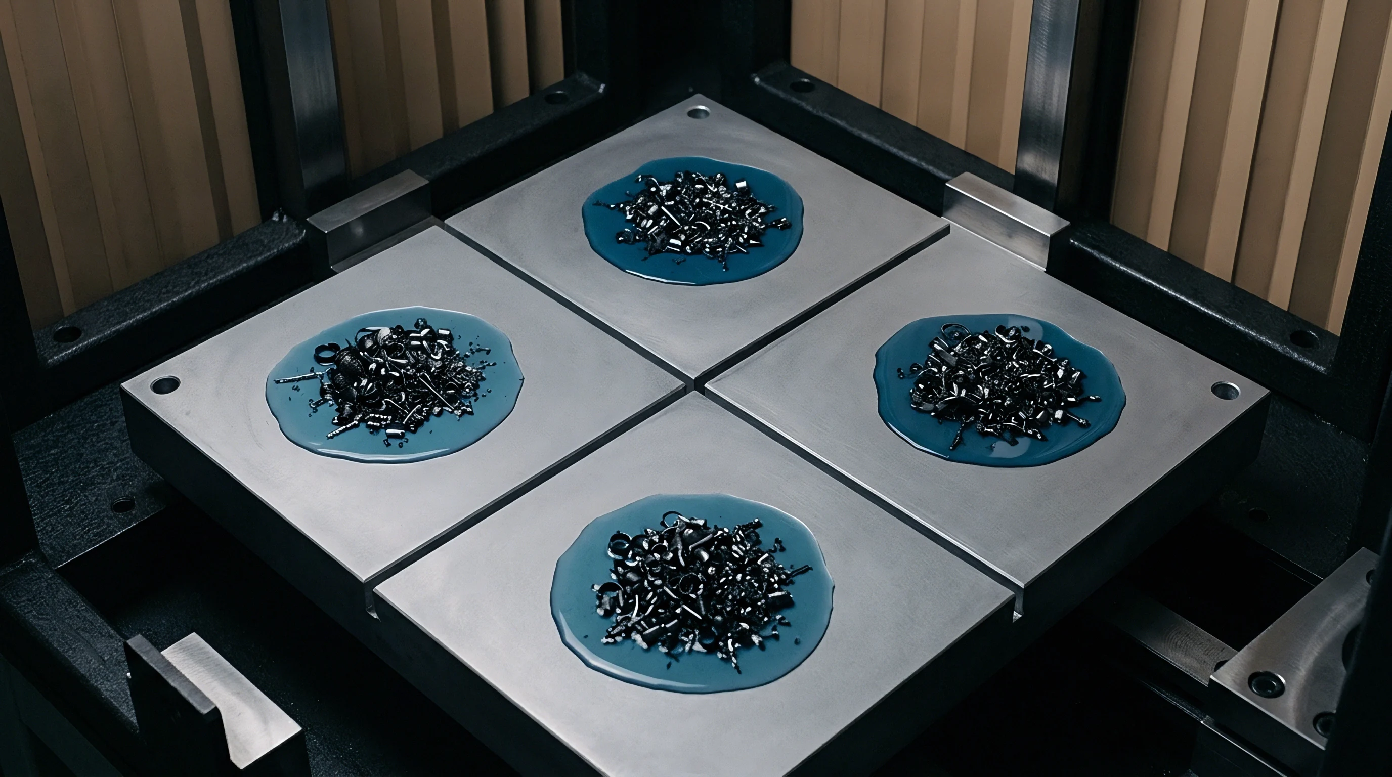
Calibrating vacancy diffusion models requires measuring material transport coefficients directly on physical samples. Generic handbook values rarely match the behavior of electrodeposited substrate copper or commercial ternary solder alloys. Trace impurities in electroplated copper ~ like sulfur, chlorine, and organic brightener residues ~ substantially alter grain boundary diffusion rates.
Empirical testing must measure actual atomic diffusion constants under controlled strain.
Advanced micro-analytical tools provide high-resolution structural and chemical data from thermal shock samples. Focused ion beam milling extracts precise cross-sectional specimens from targeted locations, such as high-stress corner interconnects. Electron backscatter diffraction maps local grain orientations to supply crystallographic input for anisotropic strain calculations, while energy-dispersive X-ray spectroscopy profiles composition across reaction zones to map elemental segregation.

Empirical Extraction of Vacancy Diffusivity Tensors
Determining stress-coupled diffusion parameters requires mechanical testing combined with tracer isotope tracking. Marker movement experiments measure asymmetric atomic drift across intermetallic couples held under fixed uniaxial tension or compression inside vacuum chambers. Inert platinum nanoparticles embedded at the original interface serve as spatial markers to track Kirkendall drift velocity under applied load.
Scanning transmission electron microscopy paired with electron energy loss spectroscopy directly measures vacancy concentrations in deformed regions. Micro-beam X-ray diffraction measures lattice parameter shifts to map localized residual stress tensors across intermetallic layers. Combining these residual strain measurements with measured elemental concentration profiles allows researchers to solve the inverse drift-diffusion equation, isolating the stress-coupling coefficient for each phase.
Incorporating IPC-TM-650 Method 2.1.1 destructive physical inspection standards into procurement agreements enforces sample extraction protocols for interfacial strain verification.

Focused Ion Beam Cross-Sectioning and Strain Mapping
Analyzing sub-micron microstructural shifts requires high-precision sample preparation. Dual-beam focused ion beam systems use gallium or xenon ion sources to cut cross-sections through specific solder joint boundaries without the mechanical deformation artifacts caused by mechanical polishing. Protective platinum or carbon coatings deposited over target zones shield delicate surface intermetallics during milling.
In Jiangsu assembly plants, slight shifts in electroplating bath chemistry alter interfacial micro-void density. High-resolution TEM of ion-milled sections shows nanoscale Kirkendall voids clustered within the Cu3Sn layer, right next to electroplated copper containing trace organic residues. Micro-diffraction mapping shows that grain boundaries perpendicular to the primary hydrostatic stress axis hold higher void volume fractions than parallel boundaries, confirming strain-coupled migration predictions.
High-resolution strain mapping techniques like nanobeam electron diffraction and precession electron diffraction measure local lattice strains down to sub-nanometer resolution. Maps across irregular intermetallic scallops reveal clear stress concentrations at scallop troughs, where lattice distortions exceed 0.8 percent strain. These strain peaks match the exact sites where vacancy condensation and micro-void growth initiate in thermal shock samples.
Uncalibrated ion-beam etching ruined five consecutive TEM foils during substrate verification.


Rupture
Vacancy condensation along irregular intermetallic boundaries triggers degradation through void nucleation and growth. As thermal shock cycling continues, stress gradients and chemical activity differences drive vacancies to critical supersaturation levels. Sub-microscopic vacancies coalesce into stable micro-voids along high-energy grain boundaries and interfaces.
This voiding reduces the load-bearing area of the joint, concentrating mechanical stress into the remaining metal and accelerating thermal fatigue rupture.
Tensile stress accelerates void growth by reducing the mechanical work needed to expand void cavities against surface energy limits. When micro-voids grow and merge along the Cu3Sn/Cu or Cu6Sn5/solder interfaces, continuous micro-cracks form. Fast thermal shock ramp rates speed up crack propagation by imposing high transient shear strains across these embrittled, void-dense intermetallic regions.

Void Nucleation and Coalescence under Extreme Temperature Swings
Kirkendall void nucleation at intermetallic interfaces depends exponentially on local vacancy supersaturation and hydrostatic tension. Classical nucleation models define the critical void radius as a function of interfacial free energy and local stress. Tensile hydrostatic stress lowers this critical radius, allowing smaller vacancy clusters to persist and grow into permanent voids.
Evaluating lead-free packaging under thermal shock reveals how strain coupling affects vacancy nucleation. Micro-CT imaging and destructive cross-sections show that void volume fractions climb sharply after an incubation period of 300 to 500 thermal cycles. Coalescence converts isolated spherical voids into continuous planar void sheets, embrittling the joint and shifting failure from ductile solder tearing to brittle interfacial cleaving under mechanical shock or vibration.
| Thermal Shock Profile | Temperature Range (°C) | Dwell Time (min) | Ramp Rate (°C/min) | Mean Cycles to Interfacial Rupture | Interfacial Void Area Fraction at Failure (%) |
|---|---|---|---|---|---|
| Standard Commercial | -40 to +125 | 15 | 15 | 2,450 | 28.4 |
| Extended Automotive | -55 to +150 | 10 | 35 | 1,120 | 32.1 |
| Extreme Aerospace | -65 to +175 | 5 | 50 | 410 | 37.6 |

How Does Nickel Concentration Suppress Kirkendall Void Nucleation?
Interfacial nickel alloying alters diffusion pathways and suppresses void nucleation. Adding nickel to copper substrates ~ or using electroless nickel immersion gold finishes ~ slows the rapid diffusion of copper into tin solder matrices. Restricting this asymmetric copper transport reduces net vacancy injection into the substrate interface.
The 85 megapascals critical hydrostatic tension threshold for spontaneous Kirkendall void nucleation comes from molecular dynamics simulations of 200,000-atom ternary cells calibrated in 2022. Dropping the thermal shock ramp rate from 40 degrees Celsius per minute to 10 degrees Celsius per minute reduces local stress accumulation, raising the effective nucleation threshold above 110 megapascals.
Nickel atoms substitute for copper in the Cu6Sn5 lattice to form (Cu,Ni)6Sn5, creating a diffusion barrier that stabilizes the interfacial layer. This phase suppresses formation of the vacancy-prone Cu3Sn phase and alters stress development across the joint. As a result, joints with nickel-bearing finishes or nickel-doped solders show far lower Kirkendall void densities during extended thermal shock testing.

Micro-Crack Propagation along Scallop Troughs
Interfacial micro-cracks propagate along paths defined by geometry and local vacancy density. Scalloped Cu6Sn5 morphology creates natural stress concentrators at scallop troughs, where models show hydrostatic tension peaking directly beneath the valley floors to create zones of rapid vacancy accumulation.
Micro-cracks initiate in void-dense zones at scallop bases and advance along the Cu3Sn interface. Under thermal shock, cyclic shear strains drive mode II fracture along these pre-damaged paths. Complete failure occurs when individual micro-cracks link across the joint width, causing open circuits or severe thermal resistance spikes in high-power semiconductor packages.
Structural degradation pathways across irregular ternary intermetallic interfaces include:
- Interfacial Kirkendall Voiding where asymmetric copper diffusion leaves vacancy clusters inside the planar Cu3Sn phase next to substrate copper.
- Scallop Trough Stress Concentration where irregular IMC geometry amplifies hydrostatic tension, accelerating local vacancy condensation under thermal cycling.
- Gold Embrittlement Fracture where dissolved gold plating forms brittle (Au,Ni)Sn4 compounds that initiate high-strain micro-cracks.
- Phase-Boundary Cleaving where thermal expansion mismatch between adjacent Cu6Sn5 and Cu3Sn crystals generates localized shear stress, tearing void-rich phase boundaries apart.
Thicker nickel barriers consistently extend thermal shock lifespan by slowing asymmetric copper transport across intermetallic boundaries.


Assembly
Applying strain-coupled vacancy models to production requires tight process control across assembly lines. Packaging facilities in Guangdong and Jiangsu rely on strictly controlled reflow profiles and plating chemistry to ensure joint reliability. Substrate finish uniformity, solder paste consistency, and surface cleanliness dictate initial intermetallic morphology; uncontrolled variables produce irregular growth that creates severe stress concentrators.
Substrate quality dictates long-term joint survival. Electroplated copper on circuit boards or direct bonded copper ceramic substrates varies in grain structure and impurity content. When electroplating baths operate with unmonitored organic additives like polyethylene glycol brighteners or levelers, codeposited organic residues collect at intermetallic boundaries during reflow.
These residues act as nucleation sites for Kirkendall voids, bypassing the initial incubation phase and accelerating failure in the field.

Process Variables Governing Interface Planarization
Achieving uniform intermetallic growth requires tight control over liquid-state kinetics during reflow. Peak temperature, time above liquidus, and cooling rate dictate early Cu6Sn5 scallop growth. Extended time above liquidus produces thick, irregular scallops with deep strain-concentrating troughs, whereas rapid cooling yields finer, flatter intermetallic layers that distribute thermal stress more evenly.
Auditing supplier line logs requires reviewing temperature ramp rates across multi-zone reflow ovens. Cooling rates above 4 degrees Celsius per second suppress coarse scallop growth and yield finer intermetallic grains. Fine-grained structures accommodate expansion strains through grain boundary sliding, reducing stress buildup and slowing vacancy drift during thermal cycling.
Process audits require reflow cooling rates above 4 degrees Celsius per second to enforce fine-grained intermetallic growth and suppress non-uniform scallop formation.

Audit Protocols for Plating Bath Organics and Impurities
Controlling interfacial voiding requires thorough auditing of substrate electroplating. Industrial copper baths use organic additives to ensure uniform deposition across micro-vias and traces, but without strict chemical control, these organic molecules break down and incorporate into the copper matrix.
Audit protocols must mandate regular chemical analysis of plating solutions using cyclic voltammetric stripping and high-performance liquid chromatography to catch bath drift. Substrate suppliers should be required to maintain copper purity above 99.95 percent, with strict caps on codeposited sulfur, carbon, chlorine, and hydrogen impurities.
Qualifying substrate manufacturing lines for high-reliability applications involves a four-step audit procedure across tier-one packaging suppliers.
- Plating Chemistry Verification requires checking bath analysis records for organic additive concentrations to confirm that leveler and brightener ratios stay inside process windows.
- Substrate Purity Testing requires secondary ion mass spectrometry on raw copper lots to confirm co-deposited carbon and sulfur remain under 10 parts per million.
- Reflow Thermal Profiling requires verifying multi-zone oven configurations with calibrated thermocouple arrays to ensure peak reflow temperatures and cooling rates hit specification.
- Interfacial Baseline Inspection requires microstructural evaluation of reflowed samples via cross-sectional electron microscopy to measure intermetallic thickness and scallop amplitude.
Writing IPC-6012 Section 3.6.2.5 mandatory cross-sectioning standards into purchase orders shifts financial liability for latent micro-void defects directly onto the substrate supplier.


Warranty
Interfacial failures driven by strain-coupled vacancy migration create major financial liabilities for electronics OEMs in high-reliability markets. Modules in harsh environments ~ such as automotive traction inverters or aerospace avionics ~ carry long warranty periods. When intermetallic interfaces fail under thermal shock, problems show up months or years into service, where field replacement, teardowns, and customer remediation multiply overall costs.
Rework costs jump once modules are encapsulated. Quantifying true operational risk requires building physics-of-failure models directly into commercial supply agreements. Standard temperature cycling tests routinely miss strain-assisted vacancy migration, so procurement contracts need to tie supplier warranty obligations directly to validated microstructural degradation models.

Financial Exposure Models for Interfacial Fatigue
Calculating the true cost of interfacial reliability defects requires modeling warranty exposure over the full product lifecycle. Landed cost models must factor in production costs alongside potential field failure liabilities, recall expenses, and consequential damages. A single batch of modules with poor substrate plating can trigger widespread field failures that wipe out any initial component savings.
Industry literature often quotes a nominal 4 percent assembly defect allowance for high-power module solder joints exposed to extended thermal shock, though missing batch-level plating histories make that figure difficult to verify across arbitrary lots. Given that uncertainty, a prudent buyer caps supplier liability allocations at 1.5 times replacement component costs while mandating destructive physical analysis on every fifth production lot.
| Oversight Regime | Initial Quality Audit Investment ($) | Predicted 5-Year Thermal Shock Field Return Rate (%) | Direct Rework and Replacement Cost ($) | Total Landed Operational Exposure ($) |
|---|---|---|---|---|
| Unmonitored Supplier | 0 | 4.2 | 630,000 | 630,000 |
| Third-Party Certificate Audit | 12,000 | 1.8 | 270,000 | 282,000 |
| Full-Time Resident Engineer | 65,000 | 0.2 | 30,000 | 95,000 |

Structuring Rework Covenants in Supply Contracts
Protecting commercial interests requires writing explicit physics-based quality standards into supply agreements. Standard purchase contracts rely on general warranty language about merchantability, leaving buyers vulnerable when latent voiding leads to field failure. Contracts should set strict microstructural acceptance criteria, including limits on intermetallic thickness, scallop roughness, and Kirkendall void volume fractions.
Releasing tooling budgets should depend on writing explicit interfacial void limits into purchase agreements. Supply agreements should require batch-level chemical certificates for substrate electroplating lines and include clear cost-allocation covenants for embrittlement failures. If destructive analysis of field returns shows void volume fractions exceeding contract thresholds, the supplier bears full liability for recall and rework costs.
Establishing contractually enforced burn-in profiles aligned with strain-coupled diffusion kinetics protects capital investments before assemblies enter automotive and aerospace service.