
Arrhenius Solid State Diffusion Parameters for Lead Free PCB Surface Finishes
Solid-state diffusion parameters dictate lead-free PCB surface finish shelf life, intermetallic growth, and solder joint reliability under thermal exposure.
Solid-state diffusion parameters dictate lead-free PCB surface finish shelf life, intermetallic growth, and solder joint reliability under thermal exposure.

Controlling interfacial intermetallic growth requires optimizing reflow profiles, selecting microalloyed solder alloys, and auditing substrate copper plating quality.
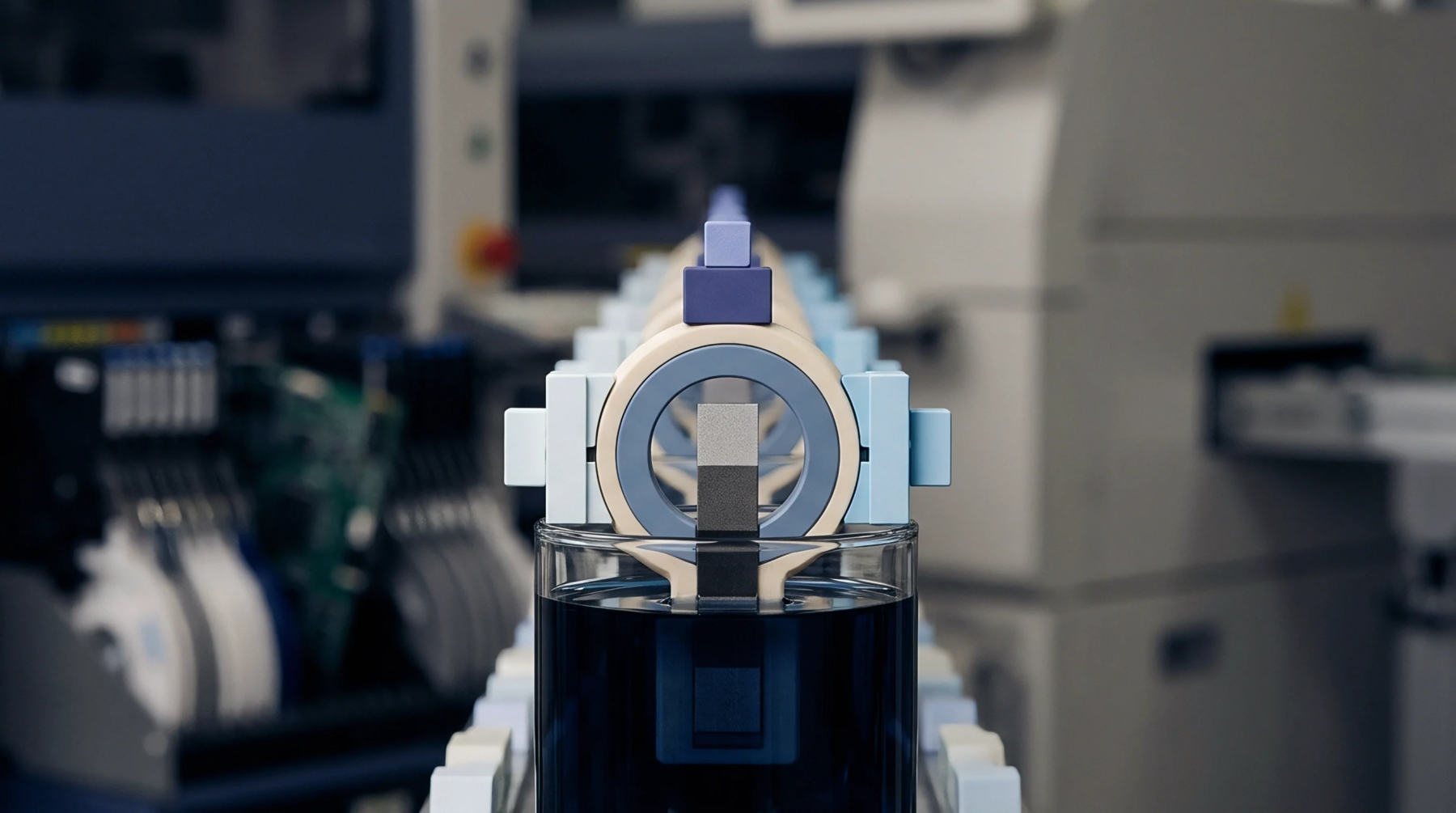
Hydrostatic stress gradients accelerate vacancy condensation in micro bumps, demanding coupled thermo-mechanical qualification to prevent field fatigue fractures.

Calibrate intermetallic vacancy growth by quantifying Cu3Sn void area fractions via focused ion beam milling across discrete thermal stress readouts.
Thermal cycling degrades lead-free solder through interfacial intermetallic growth and dynamic recrystallization, which controlled reflow cooling and micro-alloying mitigate.

Quantifying interfacial intermetallic growth kinetics under thermal aging enables accurate interconnect lifetime predictions and prevents field failures.

Solid-state intermetallic growth follows parabolic diffusion kinetics governed by Arrhenius thermal activation, requiring barrier finishes like ENIG or ENEPIG to limit brittle interface thickening and prevent Kirkendall void failures in extended service.

Steep thermal gradients across fine-pitch microbumps drive directional vacancy migration, requiring strict interface metallurgy controls and thermal gradient modeling to prevent open failures.

Submicron solder joint reliability requires capping electroplated copper sulfur content below 5 ppm and restricting aging Cu3Sn void area fractions under 5 percent.

Lead-free solder intermetallic layer growth follows parabolic solid-state diffusion kinetics, requiring strict reflow temperature control and micro-alloying to prevent embrittlement.

Intermetallic growth kinetics govern solder joint longevity; controlling thermal profiles and surface plating thickness prevents brittle interfacial failure.
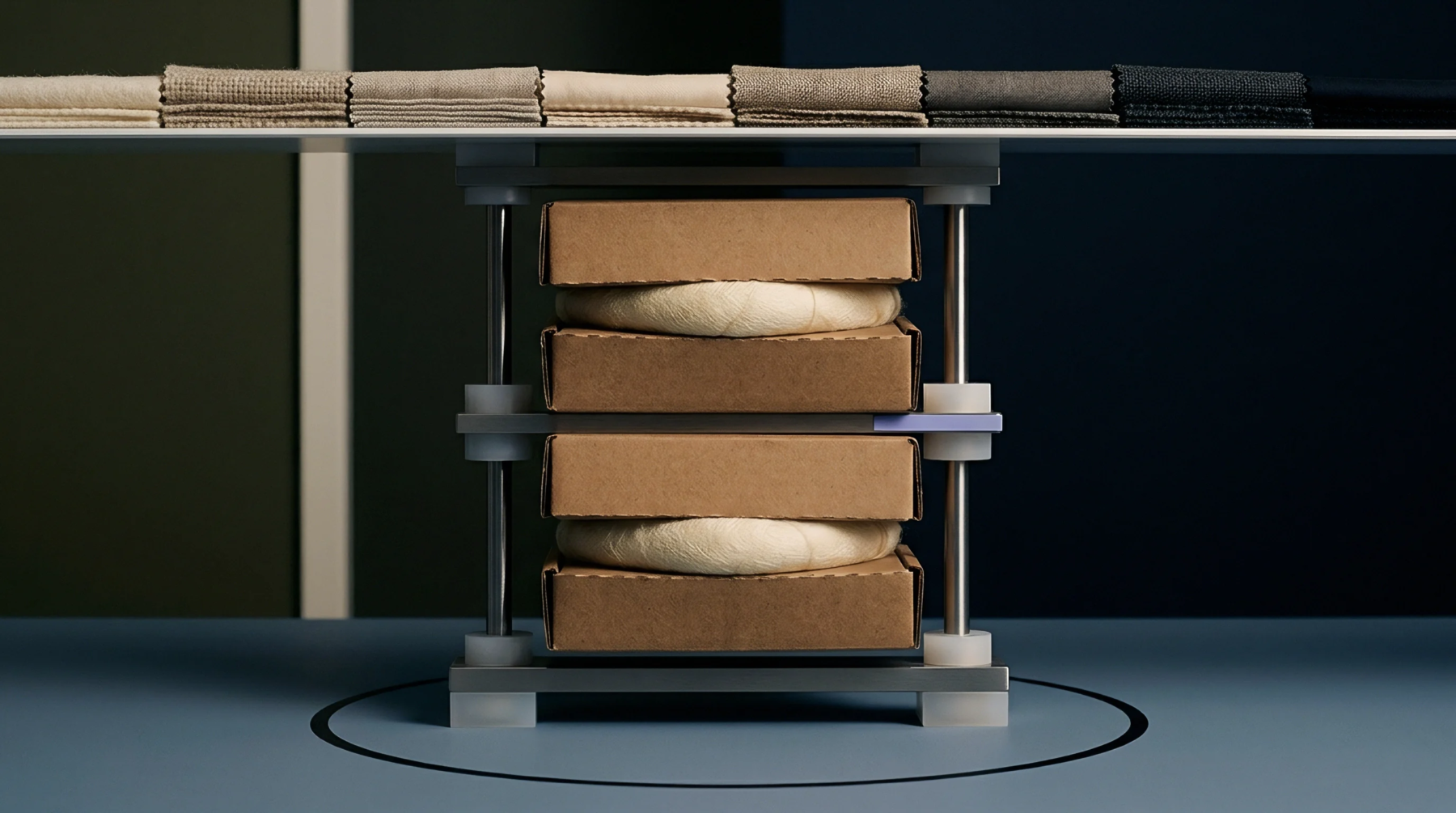
Post-holiday wave solder defects stem from pot contamination, substrate moisture, and profile drift; lab microsectioning and strict lot debits prevent field failures.

Thermal aging drives intermetallic growth and Kirkendall voiding in lead-free interfaces; controlling copper pad purity and reflow profiles prevents brittle failure.
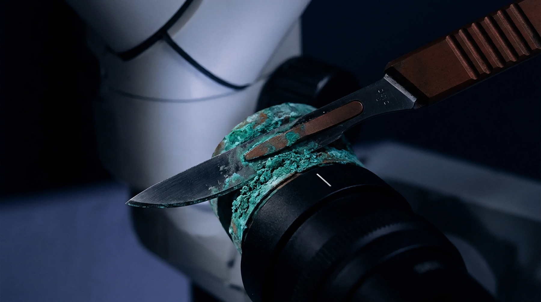
Modeling intermetallic vacancy fluxes allows engineers to suppress Kirkendall voiding and extend solder joint lifetime through targeted micro-alloying.
Expertise is a utility, not a secret. sentiention™ publishes its working knowledge as open reference: intelligence layer covering the materials it sources, the markets it enters, and the reference that serves both.