Intermetallic Growth Kinetics in Solder Joint Reliability Testing
Intermetallic growth kinetics govern solder joint longevity; controlling thermal profiles and surface plating thickness prevents brittle interfacial failure.


Crust
Intermetallic growth at the solder joint interface establishes the primary failure boundary for surface-mount electronics exposed to thermal cycling and mechanical shock. During reflow, molten tin-based solder reacts immediately with the copper substrate or surface plating, forming a metallurgical bond made up of discrete chemical phases. In standard lead-free soldering with tin-silver-copper alloys like SAC305, this liquid-solid reaction forms a thin layer of eta-phase copper-tin intermetallic (Cu6Sn5).
As boards pass through wave or reflow ovens, this initial layer develops in seconds above the alloy liquidus, creating a continuous boundary typically 0.5 to 1.5 micrometers thick. This interface changes permanently during downstream thermal processing, burn-in testing, and field operation ~ shifting from a helpful metallurgical bridge to a brittle failure site if thermal exposure goes unmanaged.
Solder joint strength depends directly on the shape and thickness of this interface. Beneath the initial Cu6Sn5 layer, solid-state diffusion under heat consumes substrate copper and forms a secondary, copper-rich epsilon-phase layer (Cu3Sn). Growing between the copper pad and the Cu6Sn5 crystals, this secondary layer has lower ductility and a different coefficient of thermal expansion than the surrounding matrix.
When the combined intermetallic layer exceeds 4 micrometers in total thickness, stress at the interface shifts from distributed shear to localized cleavage. Under mechanical drop tests or thermal shock, cracks initiate mostly along the Cu3Sn/copper pad interface or along the boundary between the Cu3Sn and Cu6Sn5 phases.
| Intermetallic Phase | Chemical Formula | Crystal Structure | Elastic Modulus (GPa) | Typical Reflow Thickness (µm) | Post-Aging Limit (µm) |
|---|---|---|---|---|---|
| Eta Phase | Cu6Sn5 | Monoclinic / Hexagonal | 85.0 | 0.5 – 1.2 | 2.5 – 4.0 |
| Epsilon Phase | Cu3Sn | Orthorhombic | 108.0 | 0.1 – 0.3 | 1.0 – 2.0 |
| Nickel-Tin Phase | Ni3Sn4 | Monoclinic | 133.0 | 0.2 – 0.6 | 1.2 – 2.2 |
| Ternary Phase | (Cu,Ni)6Sn5 | Hexagonal | 98.0 | 0.4 – 1.0 | 1.8 – 3.0 |
Surface finish selection dictates the reaction path and resulting phase sequence. Direct assembly onto bare copper protected by Organic Solderability Preservatives produces the standard dual-layer Cu6Sn5 and Cu3Sn structure. Electroless Nickel Immersion Gold finishes introduce a nickel barrier that alters diffusion dynamics entirely, slowing tin migration into the substrate while generating a thin Ni3Sn4 layer.
When tin-silver-copper solders bond to nickel finishes, copper dissolved from the solder sphere migrates to the interface, replacing nickel atoms to form a ternary (Cu,Ni)6Sn5 compound. This ternary phase suppresses brittle nickel-rich compounds as long as copper concentration in the solder matrix stays above 0.5 percent by weight. If copper depletes locally during rework reflows, phosphorus from the electroless nickel plating accumulates behind the intermetallic layer, precipitating a brittle nickel-phosphorus phase (Ni3P) that leads to interfacial delamination under impact loading.
Initial reflow process windows set the baseline for all subsequent reliability testing. Overheating extends the time above liquidus past safe limits, dissolving excess substrate metal and forming coarse, scalloped intermetallics that concentrate strain. Insufficient peak temperatures or short liquidus times leave unreacted flux trapped in micro-valleys, creating microscopic voids before thermal stress testing even starts.
Facilities in humid environments frequently run into oxidation on exposed copper traces before flux activates, resulting in patchy intermetallic coverage across the pad. An incomplete layer forces operational current and mechanical load through narrow contact points, driving rapid localized thickening during burn-in.
The formation of interfacial Cu3Sn during high-temperature storage consumes substrate copper while generating sub-micron lattice vacancies that coalesce into mechanical cleavage planes.
Measuring intermetallic thickness alone is not enough to predict joint life under load. Microstructural geometry matters just as much: planar intermetallic layers resist impact fatigue far better than irregular scalloped shapes because stress distributes evenly across the pad interface. As isothermal aging continues, the initial scalloped Cu6Sn5 crystals flatten into a continuous sheet while the underlying Cu3Sn layer thickens predictably through solid-state atomic transport.
Tracking growth rates for both phases across temperature steps gives the activation energy governing interface changes, allowing reliability engineers to project field lifespan from high-temperature storage data.
Global supply chains often misinterpret growth data by failing to separate reflow-driven intermetallic thickness from thermal growth caused by storage. Offshore assembly lines frequently report total intermetallic thickness measured right after reflow without documenting conveyor speeds or true peak temperature dwell times from thermal profilers. When test specifications require isothermal aging at 150 degrees Celsius for 1000 hours, boards arriving with pre-thickened intermetallics fail prematurely in the cycle, distorting calculated activation energy models.
Separating initial process formation from solid-state kinetic growth demands baseline cross-sectioning before environmental chambers start their thermal runs.
What specific ratio of Cu3Sn to Cu6Sn5 layer thickness marks the transition point where thermal fatigue shifts from ductile bulk solder shear to brittle interfacial fracture across different surface finishes?

Diffusion
Solid-state atomic migration drives steady intermetallic growth once the solder joint drops below its solidus temperature. Thermally activated diffusion takes place as tin atoms migrate inward toward the substrate metal while copper or nickel atoms diffuse outward into the bulk solder matrix. Modeling this phase growth relies on classical Fickian kinetics, where total intermetallic thickness scales with the square root of time under isothermal conditions.
Growth thickness at any given time follows the empirical diffusion equation:
d(t) = d_0 + (D t)^n
Here, d(t) represents total intermetallic thickness at time t, d_0 is the initial post-reflow thickness, D is the effective intermetallic diffusion coefficient at the operating or test temperature, and n is the time exponent. For pure volume diffusion through a homogeneous polycrystalline lattice, the theoretical time exponent is 0.5. Variations from 0.5 point to competing transport mechanisms: an exponent near 0.33 indicates grain boundary diffusion along microstructural paths, while values approaching 1.0 signal reaction-controlled kinetics where interface reaction rates outpace atomic transport.
The temperature dependence of the intermetallic diffusion coefficient follows an Arrhenius relationship across standard test ranges:
D(T) = D_0 exp(-Q / (R T))
In this relation, D_0 is the pre-exponential frequency factor in square meters per second, Q is the activation energy for intermetallic growth in Joules per mole, R is the universal gas constant (8.314 Joules per mole-Kelvin), and T is absolute temperature in Kelvin. Extracting these kinetic constants requires isothermal aging experiments across at least three temperature setpoints ~ typically 125, 150, and 175 degrees Celsius. Plotting the natural logarithm of the parabolic growth rate against reciprocal absolute temperature produces a line with a slope equal to negative activation energy divided by the gas constant.
| Substrate Finish | Dominant Growing Phase | Activation Energy Q (kJ/mol) | Pre-exponential D0 (m²/s) | Time Exponent n | 150°C Growth Rate (µm/√h) |
|---|---|---|---|---|---|
| Bare Copper (OSP) | Cu6Sn5 + Cu3Sn Total | 84.5 | 3.2 x 10^-7 | 0.48 | 0.085 |
| Bare Copper (OSP) | Cu3Sn Phase Isolated | 106.2 | 1.5 x 10^-5 | 0.51 | 0.032 |
| ENIG (Ni-P/Au) | Ni3Sn4 | 112.0 | 8.8 x 10^-5 | 0.42 | 0.019 |
| ENEPIG (Ni-Pd-Au) | (Pd,Ni)Sn4 / Ni3Sn4 | 124.8 | 4.1 x 10^-4 | 0.39 | 0.012 |
Kirkendall voiding is a serious structural risk caused by unbalanced solid-state diffusion. In copper-tin couples, copper diffuses outward into the Cu3Sn layer faster than tin moves inward toward the copper substrate. This mismatch produces a net flux of atomic vacancies toward the copper substrate interface.
Once non-equilibrium vacancies exceed thermal saturation limits, they condense into micro-voids along the boundary between the copper pad and the Cu3Sn phase. Prolonged heat above 100 degrees Celsius accelerates this voiding, turning a dense metallic interface into a porous lattice vulnerable to failure under low-energy mechanical impacts.
Substrate impurities and plating additives strongly affect Kirkendall void density. Sulfur, hydrogen, and organic brighteners trapped in electroplated copper during board fabrication serve as nucleation sites for vacancies. Electroplated copper with high internal stress or fine grains below 1 micrometer accelerates vacancy buildup compared to coarse-grained rolled-annealed foil.
When working with offshore board suppliers, auditing plating bath chemistry and annealing procedures is just as critical as checking alloy compositions; contaminated copper deposits can double Kirkendall voiding rates under the same thermal exposure.
Excessive intermetallic growth alters stress distribution in fine-pitch BGA solder spheres. As ductile solder converts to stiff intermetallic compound, the volume of compliant solder shrinks, reducing standoff height between component and board. This drop in standoff height increases shear strain during thermal expansion mismatches between package and PCB.
On micro-BGA packages with pads under 250 micrometers, intermetallic growth can consume up to 30 percent of original solder volume within 1000 hours at 125 degrees Celsius, shifting compliance burdens onto the underfill.
Calculating activation energy from empirical cross-sections across multi-temperature stress runs evaluates atomic diffusion dynamics. When activation energies drop below 70 kilojoules per mole, non-bulk mechanisms like grain boundary sliding or micro-cracking take over, signaling poor initial microstructures or excessive local strain during testing.
Diffusion accelerates non-linearly when current flows during thermal stress ~ a phenomenon known as electromigration. Current densities above 10,000 Amperes per square centimeter exert an electron wind that forces metallic ions toward the anode end of the joint. This directional transport causes rapid, asymmetric intermetallic accumulation at the anode pad and heavy voiding and depletion at the cathode pad.
Electromigration-driven growth runs up to five times faster than isothermal thermal aging, requiring dedicated test layouts with isolated routing to separate current-driven phase changes from thermal kinetics.
Doubling intermetallic layer thickness under pure volume diffusion conditions requires a fourfold increase in thermal exposure time.

Specimen
Test vehicle design determines whether intermetallic growth data from environmental testing is actually valid. Standard commercial boards have trace geometries and thermal paths that create parasitic thermal gradients, causing localized variations in intermetallic thickness. Dedicated reliability vehicles use standardized daisy-chain patterns following IPC-9701 and IPC-9704 guidelines.
These boards isolate individual component loops for continuous four-wire Kelvin resistance monitoring while preserving thermal uniformity across all pads inside the test chamber.
Solder mask definition sets the boundary conditions for intermetallic distribution across the pad. Non-Solder Mask Defined (NSMD) pads expose copper sidewalls to molten solder during reflow, allowing the intermetallic layer to anchor around the trace perimeter. This provides a larger surface area, distributing shear stress across a wider interface and lowering net growth per unit area.
Solder Mask Defined (SMD) pads restrict solder contact to the top pad surface, creating a sharp stress concentration notch at the mask edge where intermetallic growth drives crack propagation under fatigue.
Trace geometry, copper foil weight, and dielectric stackup must be tightly specified before building test coupons. Changes in copper thickness from 0.5 ounce (17.5 micrometers) to 2.0 ounces (70 micrometers) alter pad thermal mass enough to shift reflow peak temperatures by up to 8 degrees Celsius if furnace profiles are left unadjusted. That temperature variation changes initial post-reflow thickness across different parts of the same board.
Standardizing test vehicles on a four-layer FR-4 High-Tg substrate with uniform 1.0-ounce copper across all layers eliminates these thermal mass differences and yields consistent baseline intermetallics.
Plating specifications require tight thickness tolerances to prevent unwanted phase transformations. Electroless Nickel Immersion Gold demands a nickel deposit between 3.0 and 6.0 micrometers and immersion gold held to 0.025 to 0.075 micrometers. Gold thickness above 0.1 micrometer leads to embrittlement, where dissolved gold forms brittle AuSn4 needles that drift to the interface during cooling.
Conversely, nickel under 2.5 micrometers risks complete consumption over multiple reflows, allowing tin to attack the underlying copper trace directly and form unstable, porous ternary compounds.
- Substrate Material Receipt requires chemical verification of resin glass transition temperature exceeding 170 degrees Celsius via Differential Scanning Calorimetry and proof of decomposition temperature above 340 degrees Celsius.
- Copper Surface Preparation requires micro-etching to remove at least 1.2 micrometers of surface copper, followed by atomic absorption spectroscopy confirming surface ionic cleanliness below 0.75 micrograms per square centimeter sodium chloride equivalent.
- Metallic Plating Application requires X-ray Fluorescence testing across 15 points per panel to confirm electroless nickel thickness within 3.5 to 5.0 micrometers and immersion gold within 0.03 to 0.05 micrometers.
- Solder Paste Printing requires laser-cut electro-polished stainless steel stencils with 100 percent aperture area ratio verification using 3D automated optical inspection to keep paste volume variance below 5 percent across all daisy-chain pads.
- Reflow Thermal Profiling requires real-time thermocouple capture confirming peak temperatures between 238 and 245 degrees Celsius, with total time above liquidus (217 degrees Celsius) held between 60 and 75 seconds.
Assembly of test vehicles demands tight control over oven atmospheres and cooling rates. Reflowing under nitrogen with under 50 parts per million oxygen cuts oxidation, reducing void formation in the intermetallic layer by over 40 percent compared to air reflow. Post-reflow cooling rate sets the starting grain size for both bulk solder and growing intermetallic crystals.
A cooling rate between 2.5 and 4.0 degrees Celsius per second suppresses coarse primary Cu6Sn5 needles in the solder matrix, yielding a uniform interfacial layer that passes baseline inspection.
Specifying non-solder mask defined pads with controlled copper sidewall etching reduces interfacial stress concentration by distributing intermetallic growth across a 20 percent larger surface area.
Component selection for test vehicles must match the exact alloy, plating, and package architecture of production hardware. Using dummy parts with solid copper leadframes instead of silicon dies distorts stress modeling, since thermal expansion mismatch between silicon and organic substrates drives localized shear strain that accelerates intermetallic growth. Test coupons need real component packages with factory ball alloys matching production specs so that trace additions like bismuth, nickel, or micro-alloyed titanium function within their intended kinetic inhibition windows.
Failing to standardize solder paste volume across test pads causes wide variations in bulk-solder-to-intermetallic ratios, skewing calculated degradation rates and passing parts that will fail in the field.
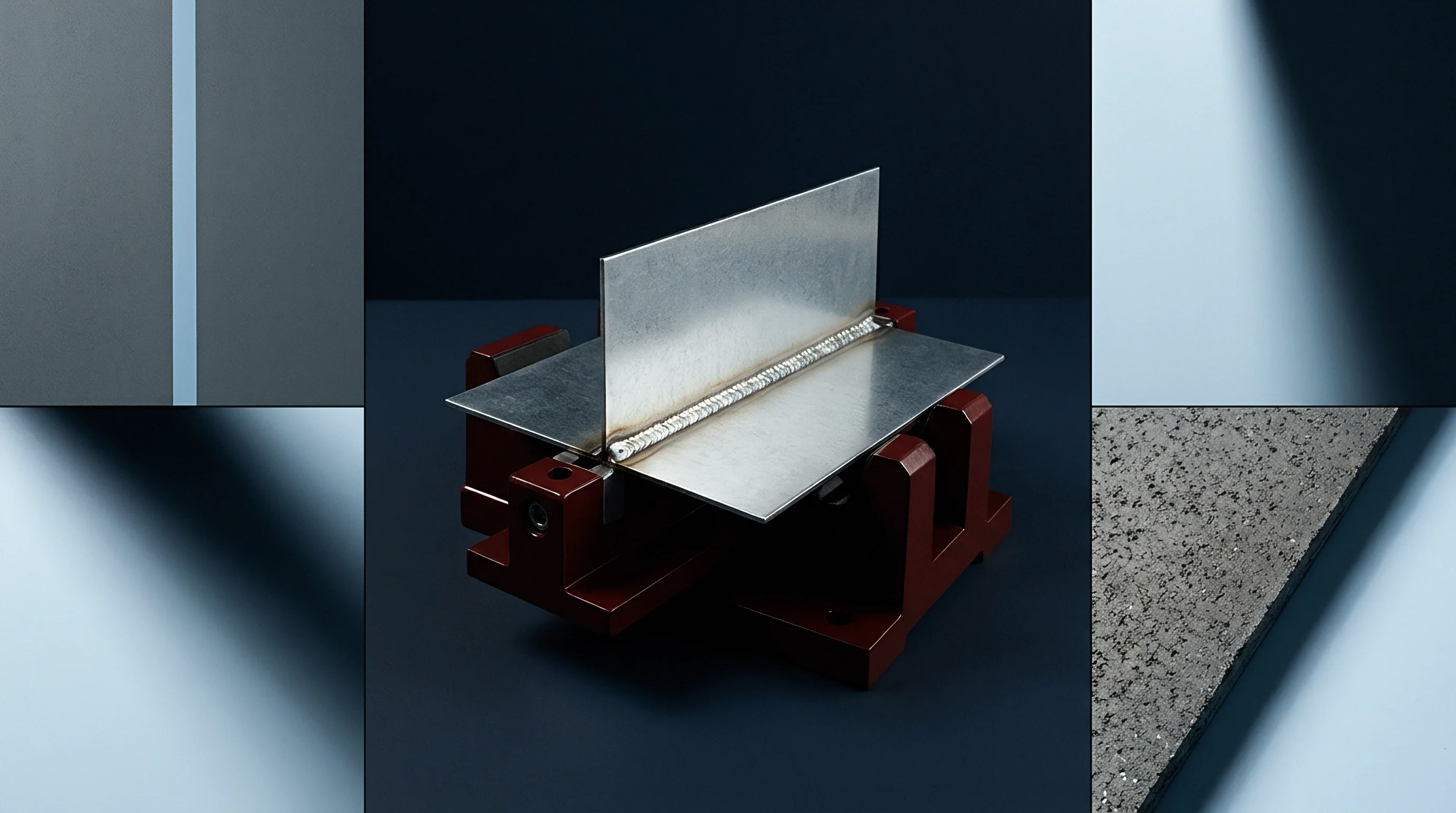
Aging
Thermal aging protocols isolate heat-driven diffusion kinetics from mechanical fatigue. Isothermal aging requires placing assembled, baseline-inspected vehicles into environmental chambers that maintain temperature within plus or minus 0.5 degrees Celsius throughout the internal volume. Standard test schedules call for exposure intervals at 100, 250, 500, 750, and 1000 hours.
Pulling sample sets at each interval allows step-by-step measurement of intermetallic growth, letting engineers plot thickness against the square root of time to calculate diffusion coefficients for specific production lots.
Isothermal aging setpoints must stay below the solder alloy’s solidus temperature to prevent melting or artificial microstructural coarsening. For SAC305 (solidus of 217 degrees Celsius), aging profiles are run at 125, 150, and 175 degrees Celsius. The 175-degree temperature provides aggressive acceleration, growing Cu3Sn rapidly and accumulating Kirkendall voids within 250 hours.
Aging at 125 degrees Celsius reflects long-term operating conditions, offering the baseline kinetic data needed to verify whether high-temperature models accurately predict field life.
| Aging Temperature (°C) | Target Exposure Intervals (Hours) | Primary Phase Monitored | Acceleration Factor (vs 55°C Field) | Critical Failure Metric |
|---|---|---|---|---|
| 100 | 250, 500, 1000, 2000 | Cu6Sn5 Growth | 8.5x | IMC Thickness > 3.0 µm |
| 125 | 100, 250, 500, 1000 | Cu3Sn Nucleation | 28.4x | Phase Ratio Cu3Sn/Cu6Sn5 > 0.4 |
| 150 | 48, 100, 250, 500, 1000 | Kirkendall Voiding | 86.2x | Void Line Density > 25% boundary |
| 175 | 24, 48, 100, 250, 500 | Substrate Cu Depletion | 235.0x | Complete Plating Consumption |
Thermal cycling introduces expansion mismatch stresses that act alongside intermetallic phase growth. Standard profiles following JESD22-A104 call for swings from minus 40 to plus 125 degrees Celsius, with 15-minute dwells at each extreme and ramp rates of 10 degrees Celsius per minute. Cycling degrades joints faster than static isothermal aging because alternating shear strains crack the brittle Cu6Sn5 crystal lattice.
These micro-cracks serve as fast transport paths, letting unreacted tin bypass the intermetallic barrier and react directly with substrate copper to accelerate growth under strain.
Controlling chamber airflow and board orientation prevents thermal gradients during long test runs. High-velocity forced air keeps temperatures uniform across all positions, whereas stagnant pockets can cause 5-degree Celsius offsets between central and outer test coupons. At a 150-degree setpoint, a 5-degree error skews calculated diffusion rates by roughly 12 percent ~ an unacceptable error for activation energy models.
Racks should hold boards parallel to airflow with at least 20 millimeters of space between panels to ensure uniform heat transfer.
Reliability protocols require continuous, real-time resistance monitoring across all daisy-chain loops during thermal aging and cycling. Spikes exceeding 20 percent above baseline for longer than 1 microsecond indicate micro-cracks along the intermetallic interface. Intermittent open circuits seen during hot dwells frequently close during cooling as thermal contraction forces crack faces back together.
Offline, post-test resistance measurements miss these transient opens completely, underreporting degradation by failing to catch interface separation in real time.
If high temperatures meet ambient humidity inside unsealed chambers, moisture degrades PCB laminates and releases volatile organic compounds that attack exposed joint perimeters. Modern testing requires sealed chambers with dry air flushes kept at dew points below minus 40 degrees Celsius. Suppressing oxidation and hydrolysis ensures that observed microstructural changes and layer growth stem purely from solid-state diffusion rather than environmental corrosion.
The aging runs completed on schedule without abnormalities, and observed joint separation proved to be the result of mechanical shock during post-test handling rather than thermal degradation of the intermetallic layer.


Sectioning
Analyzing intermetallic microstructures demands careful metallurgical preparation to prevent artificial voids, phase smearing, or polishing cracks. Cutting samples with standard abrasive wheels creates mechanical shock that fractures brittle intermetallics, ruining microscopic analysis. Initial sectioning must be done with high-precision diamond wafering saws running below 300 rpm under continuous oil coolant.
The cut line needs to stay at least 1 millimeter away from the target solder joints so grinding can remove the heat-affected, stress-damaged zone.
Epoxy potting stabilizes the delicate intermetallic interface before grinding and polishing. Ultra-low-viscosity cold-mount epoxies mixed under vacuum fill micro-cracks, surface pores, and complex package features completely. Curing should take place at room temperature over 24 hours.
Fast hot-mounting presses operating at high pressure (above 20 Megapascals) and temperature (above 150 degrees Celsius) generate artificial stress that distorts intermetallic morphology and creates false micro-voids at the interface.
Grinding and polishing require a strict progression through finer diamond abrasives to produce flat samples without edge rounding. Silicon carbide papers from 320 down to 1200 grit handle initial planarization under light hand pressure with water lubrication. Polishing then moves through polycrystalline diamond suspensions at 3.0, 1.0, and 0.25 micrometers on synthetic velvet.
A final 45-second polish with a non-crystallizing colloidal silica suspension (0.04 micrometer particle size) on a CMP pad removes surface deformation, leaving crisp boundaries between bulk solder, Cu6Sn5, Cu3Sn, and the copper pad.
Chemical etching highlights phase boundaries and grain structures for optical and electron microscopy. Immersing sections in 95 percent ethanol and 5 percent concentrated hydrochloric acid for 3 to 5 seconds selectively etches the tin-rich solder matrix, leaving Cu6Sn5 crystals standing out in clear relief. Alternatively, an ammonium persulfate etch (5 grams ammonium persulfate in 100 milliliters distilled water) attacks copper, exposing the bottom of the Cu3Sn layer to reveal Kirkendall void distribution across the interface.
Scanning Electron Microscopy in Backscattered Electron (BSE) mode is the benchmark for measuring intermetallic layers. BSE imaging creates atomic number contrast: phases with heavier elements appear brighter than lighter regions. At accelerating voltages between 15 and 20 kilovolts, the phases separate clearly by gray scale: bulk tin is bright gray, Cu6Sn5 is medium gray, Cu3Sn forms a dark gray band, and the copper pad shows as a distinct dark base.
Energy Dispersive X-ray Spectroscopy (EDS) confirms stoichiometry, verifying 6-to-5 atomic ratios for eta phase and 3-to-1 for epsilon phase.

Why Do Nickel Immersion Finishes Suffer Interfacial Voiding?
Electroless Nickel Immersion Gold finishes suffer from a specific failure known as black pad, caused by hyper-corrosion of the nickel layer during gold immersion. When gold displaces nickel in an unbuffered acidic bath, galvanic attack selectively dissolves nickel along grain boundaries, leaving a porous, phosphorus-rich layer. During reflow, solder reacts with the remaining nickel to form Ni3Sn4 but fails to wet into the corroded micro-fissures.
Thermal aging then accelerates phosphorus segregation behind the intermetallic, forming a weak Ni3P layer full of planar micro-voids that fail under mild impact.
Accurate measurement of intermetallic thickness requires image analysis software applied to high-resolution SEM micrographs. Single-point linear measurements introduce large errors because post-reflow intermetallics are scalloped and irregular. Determining true average thickness requires calculating total phase cross-sectional area along a set interface length and dividing that area by the length:
d_avg = (1 / L) integral(y(x) dx, from 0 to L)
Image analysis tools compute this integral by segmenting grayscale BSE images into binary maps, counting pixels for area, and dividing by total pad length. Reliable results require sampling at least 20 random fields per joint across a minimum of 5 joints per test condition to stay within plus or minus 5 percent statistical confidence limits.
Under Section 4.3 of IPC-TM-650, Method 2.1.1, micro-section acceptance requires polished samples to show no edge-rounding at phase boundaries, no solder smearing over intermetallic layers, and void counts evaluated along a continuous 100-micrometer interface at 5000x magnification.

Escalation
Cross-border manufacturing contracts for electronic assemblies need clear, enforceable technical limits on intermetallic phase growth. Standard purchase specifications that cite industry standards without defining specific intermetallic metrics leave buyers exposed to reliability risks from vendor process changes. Supply agreements should build maximum thickness limits, phase ratio caps, and required testing protocols directly into contract annexes.
Vendors must understand that lot acceptance depends just as much on microstructural compliance as on electrical testing.
Enforcing quality standards requires clear verification steps across production. Bare circuit boards entering assembly facilities must pass baseline solderability and plating thickness checks before component placement. Solder paste vendors must furnish lot-specific chemical certifications verifying trace element tolerances.
During full-scale production, third-party inspectors should pull quarterly samples, cross-sectioning joints after reflow to confirm that initial Cu6Sn5 stays below 1.5 micrometers and that liquidus dwell times haven’t drifted to make up for faster conveyor speeds.
When environmental stress testing uncovers early intermetallic degradation or excessive Kirkendall voiding, formal escalation procedures dictate the root-cause investigation. The buyer immediately freezes inventory from the suspect build window. Within 48 hours, the factory must produce raw thermal profiling logs, electroplating bath maintenance records, and material lot certifications for the run in question.
Independent labs receive duplicate test vehicles to replicate aging results and run high-speed impact shear testing under identical conditions.
Commercial liability clauses need to tie financial accountability to specific microstructural criteria. If intermetallic growth rates exceed kinetic models because a supplier altered plating chemistry, foil additives, or reflow profiles without authorization, the supplier absorbs all scrap, rework, air freight, and third-party lab costs. Supply agreements should state that a batch fails automatically if cross-sections reveal Kirkendall void line densities over 15 percent of the interface length after 500 hours of aging at 150 degrees Celsius.
Managing offshore assembly requires hands-on oversight of thermal profilers and metallography labs rather than relying on scanned reports. Vendors under margin pressure sometimes skip micro-sectioning or use quick manual polishing that smears soft solder over intermetallics, hiding micro-voids. Sending trained independent inspectors to audit factory labs ensures polishing gear, diamond suspensions, and SEM imaging meet standard specs.
On-site verification is the only reliable way to confirm that reported kinetic data reflects real field performance.
Establishing these routines turns metallurgical growth formulas into predictable quality controls. When suppliers know that interfacial microstructures face routine high-resolution cross-sectioning tied to financial consequences, plant engineering teams take thermal profiling and plating quality seriously. Regular oversight stabilizes assembly, keeping intermetallic growth within safety margins and protecting product reliability across global supply chains.