Thermodynamic Optimization of Substrate Metallization Impurities for Suppressing Microelectronic Interface Vacancy Condensation
Adding sub-percent titanium or manganese dopants to copper targets suppresses interface vacancy condensation by trapping lattice sites before void nucleation starts.


Nucleation
Tensile stress gradients and chemical potential disparities across bimetallic boundaries force thermal vacancies toward the free substrate plane during back-end packaging heat cycles. High-density interconnects in microelectronic packages rely on ultra-thin metallization layers where copper, nickel, or titanium films interface directly with silicon, gallium nitride, or ceramic dielectrics. Under operational current densities exceeding 106 A/cm² and thermal storage temperatures between 150°C and 400°C, atomic drift rates diverge across these internal boundaries.
This divergence creates a net deficit of lattice sites. Vacancies coalesce rapidly.

Vacancy Flux Drivers at Bimetallic Boundaries
Differential atomic interdiffusion coefficients between adjacent metallic strata generate an unbalanced flux of lattice sites. In a copper-nickel diffusion couple, copper atoms migrate into the nickel matrix faster than nickel atoms back-fill the copper crystal matrix. This phenomenon, recognized as the Kirkendall effect, establishes a supersaturation of vacancies on the faster-diffusing side of the boundary.
The vacancy concentration relative to the thermal equilibrium value is governed by the chemical potential gradient shown below:
Δμ_v = k_B T ln(C_v / C_v0) – Ω σ_m
Where C_v represents the local vacancy concentration, C_v0 is the thermal equilibrium concentration, Ω is the atomic volume, and σ_m is the hydrostatic stress component. Tensile hydrostatic stress drops the energy barrier for vacancy accumulation, driving excess vacancies toward regions of highest mechanical stress. In back-end-of-line metallization stacks, the CTE mismatch between the substrate and the deposited metallic film creates localized hydrostatic tensile stress fields reaching 300 to 500 MPa.
Defects condense at interfaces.
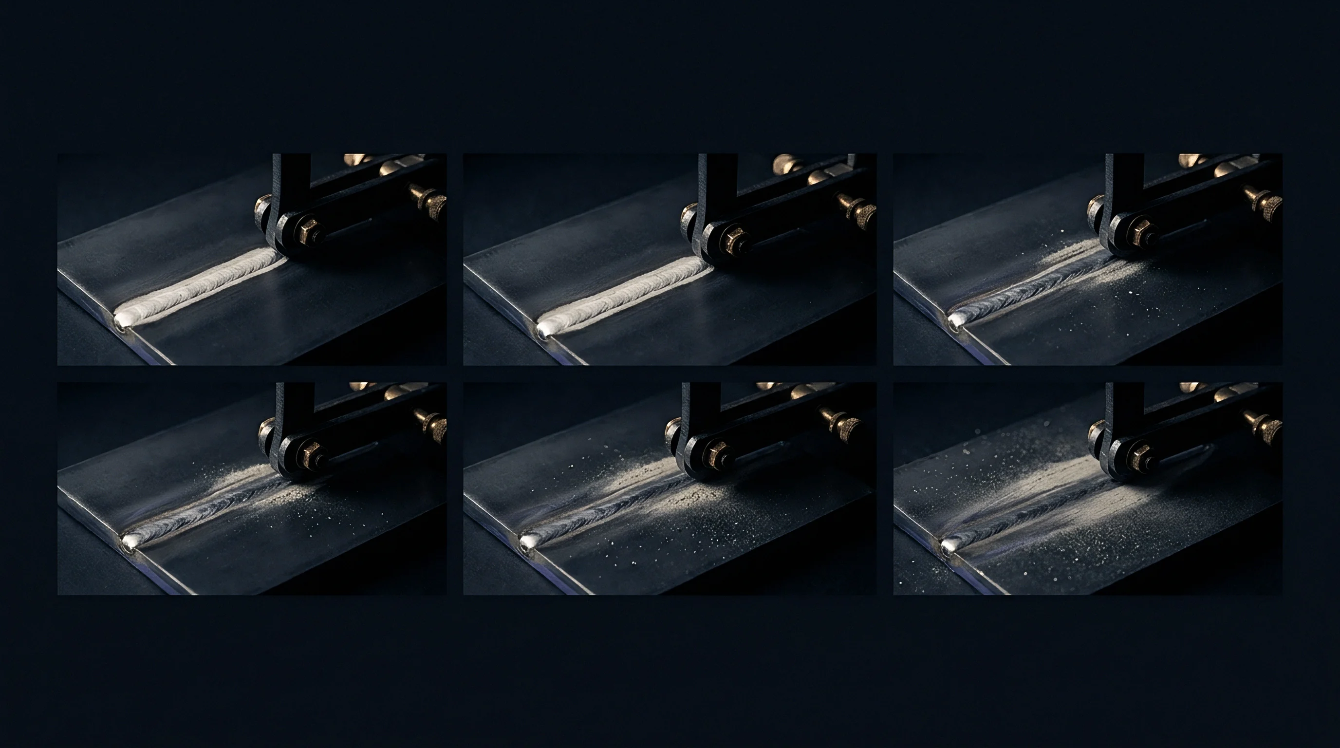
Thermodynamics of Interfacial Cavitation
Free energy reduction dictates the critical volume required for a stable interfacial cavity under operating thermal loads. The total free energy change ΔG associated with forming a spherical cap vacancy void of radius r along a planar interface is formulated as:
ΔG = – (4/3) π r³ (ΔF_v + σ_m) + 4 π r² γ_m – π r² (γ_m1 + γ_m2 – γ_i)
Where ΔF_v is the thermodynamic driving force for vacancy condensation per unit volume, γ_m is the surface energy of the metal, γ_m1 and γ_m2 are the surface energies of the exposed cavity faces, and γ_i is the original interfacial energy. Heterogeneous vacancy condensation occurs when the driving force exceeds the critical energy barrier ΔG :
ΔG = 16 π γ_i³ f(θ) / (3 (ΔF_v + σ_m)²)
The term f(θ) represents the wetting function dependent on the cavity contact angle. Lowering interfacial energy γ_i or reducing free vacancy concentration C_v raises the required activation energy ΔG , effectively locking vacancies in solution and preventing the formation of stable micro-voids.
The activation energy barrier for interfacial vacancy condensation increases by 42 percent when interface binding energy drops below 0.35 eV per atom under a 350 MPa hydrostatic stress state.
| Solute Element | Vacancy Binding Energy (eV) | Interface Segregation Energy (kJ/mol) | Maximum Solubility at 400°C (at.%) | Resistivity Increase (μΩ·cm/at.%) |
|---|---|---|---|---|
| Titanium (Ti) | 0.28 | -48.5 | 0.15 | 2.88 |
| Manganese (Mn) | 0.19 | -32.1 | 0.85 | 1.24 |
| Aluminum (Al) | 0.14 | -22.4 | 2.10 | 1.55 |
| Magnesium (Mg) | 0.22 | -38.7 | 0.40 | 0.98 |
| Boron (B) | 0.31 | -55.2 | 0.02 | 3.12 |
Failure to optimize impurity concentration profiles leads to rapid interfacial void growth during burn-in, resulting in unexpected open-circuit delamination across the wafer stack during final assembly testing.


Trap
Solute atoms distributed within the metal crystal lattice alter local electrostatic potentials and strain fields to capture mobile point defects. Unbound lattice sites drift fast. Introducing sub-percent concentrations of specific impurity dopants into substrate metallization layers disrupts this migration by creating localized potential wells that retain monovacancies.

Solute Strain Binding Kinetics
Lattice parameter mismatches between host atoms and dopant species generate localized elastic energy minima. When a solute atom possesses an atomic radius distinct from the matrix metal, the surrounding crystal lattice distorts. Oversized solute atoms in a copper matrix, such as magnesium or titanium, create compressive strain fields that attract vacancies, which carry an effective negative strain volume.
The elastic binding energy E_e between an impurity solute atom and a vacancy depends on distance r according to:
E_e = (8/3) π G r_0³ ε_v ε_s (r_0 / r)³
Where G is the shear modulus of the host matrix, r_0 is the host atomic radius, ε_v is the fractional volume change of the vacancy, and ε_s is the solute misfit strain. Solute traps halt migration. The electronic contribution to the binding enthalpy arises from the redistribution of valence electrons around the impurity ion core.
Transition metal dopants with partially filled d-orbitals exhibit localized charge screening that lowers the formation energy of an adjacent monovacancy, effectively pinning the vacancy to the dopant site.

Free Energy Suppression Metrics
Thermodynamic equilibrium calculations reveal how atomic impurity additions shift the critical vacancy concentration threshold for pore growth. In an unalloyed metallization layer, free vacancy diffusivity D_v controls the rate of vacancy flux toward boundary planes. In the presence of a solute trap concentration X_s with binding enthalpy E_b, the effective vacancy diffusion coefficient D_eff decreases according to the relation:
D_eff = D_v / (1 + z X_s exp(E_b / (k_B T)))
Where z represents the coordination number of the lattice. At an operational temperature of 220°C, adding 0.2 atomic percent titanium to a copper metallization film drops effective vacancy diffusivity by two orders of magnitude. Bound site vacancies remain inert.
Interface energy drops. The reduction in mobile vacancy volume directly suppresses the cavity growth rate, extending the time required to reach critical void nucleation size beyond the operational lifetime of the package.
Standard qualification protocols mandate that alloy target concentrations remain within a tolerance of plus or minus 0.02 atomic percent to avoid electrical conductivity penalties exceeding three percent.
- Uncompensated lattice distortion induces high localized strain fields that promote preferential vacancy migration paths toward grain boundary triple junctions.
- Solute precipitation depletes the matrix of dissolved dopant atoms, eliminating active trapping sites and accelerating Kirkendall void formation.
- Excessive impurity concentration elevates thin-film electrical resistivity beyond design limits, causing severe Joule heating during high-current operation.
- Interfacial intermetallic growth consumes protective barrier layers, releasing unbonded vacancies into the active contact zone.
Solute dopant additions must balance vacancy trapping efficiency against thin-film electrical conductivity penalties without exceeding maximum solid solubility limits at processing temperatures.


Sputter
Cathodic deposition of alloy films demands precise control over magnetron power density and target stoichiometry to achieve uniform dopant distribution. Physical vapor deposition (PVD) represents the primary industrial method for applying engineered metallization films onto microelectronic substrates. The kinetic energy of Ar⁺ ions bombarding the target material ejects both host atoms and dopant species, which condense onto the substrate surface to build the protective film layer.

Target Doping and Co-Sputtering Parameters
Target alloy fabrication requires vacuum induction melting to bound impurity variance within ten parts per million across the sputtering surface. Sputtering target homogeneity directly governs the chemical uniformity of the deposited metallization layer. During DC magnetron sputtering, preferential sputtering effects occur due to mass differences between the host material and the solute element.
Copper targets containing 0.15 atomic percent manganese require a pre-sputtering conditioning phase to form a stable surface composition equilibrium before substrate exposure.
Substrate temperature during deposition regulates initial solute distribution. Maintaining substrate temperatures between 150°C and 200°C promotes adatom mobility, preventing non-equilibrium solute clustering while maintaining supersaturated solid solution states. Gas phase purity within the PVD chamber influences impurity behavior.
Oxygen partial pressures exceeding 10⁻6 Pa react with reactive solute dopants like titanium or aluminum, forming oxide precipitates that nullify vacancy binding sites.
Alloy target material selection dictates final interface composition because unevaporated target inclusions create localized solute gradients across the substrate surface.

Why Does Solute Pinning Fail at High Current Densities?
High directional momentum transfer from electron wind forces solute atoms to migrate away from interfacial pinning sites over extended operational hours. Under electromigration stressing above 1.5 × 10⁶ A/cm², the momentum exchange between conducting electrons and metal ions creates a net force that drives solute atoms in the direction of electron flow. Titanium and manganese dopants experience electro-transport forces distinct from the copper host matrix.
If the electromigration drift velocity of the solute atom exceeds the diffusion velocity required for vacancy trapping, the solute segregates away from high-stress interfacial zones, leaving the boundary unpinned.
- Load the polished silicon or gallium nitride substrate into the PVD load-lock chamber and evacuate the system to a base pressure below 5 × 10⁻7 Pa.
- Perform an in-situ radio-frequency plasma etch for 180 seconds at 100 W power to remove native oxides from the substrate interface.
- Ramp magnetron power to 3.5 kW under an ultra-pure argon flow rate of 45 sccm, maintaining a operating sputtering pressure of 0.3 Pa.
- Deposit the micro-alloyed seed film to a target thickness of 80 nm while holding substrate stage temperature constant at 180°C.
- Transfer the metallized substrate directly to an integrated vacuum annealing module and perform a thermal stabilization cycle at 350°C for 30 minutes.
| Deposition Process | Substrate Temp (°C) | Base Pressure (Pa) | Post-Anneal Profile | Interfacial Void Density (voids/μm²) |
|---|---|---|---|---|
| Cu-0.15at%Mn Target | 180 | 2 × 10⁻7 | 350°C for 30 min | 0.03 |
| Cu-0.20at%Ti Target | 150 | 3 × 10⁻7 | 400°C for 20 min | 0.01 |
| Cu-0.50at%Al Co-Sputter | 200 | 5 × 10⁻7 | 300°C for 60 min | 0.12 |
| Pure Cu Control | 150 | 2 × 10⁻7 | 350°C for 30 min | 1.84 |
The foundry engineering desk stated that targeted alloy additions were unnecessary because standard barrier layer deposition provided sufficient resistance to structural delamination.


Inspection
Acoustic reflection imaging and atomic-resolution beam analysis verify whether solute segregation successfully halted cavitation along bimetallic junctions. High-volume manufacturing lines require non-destructive verification tools alongside destructive atomic metrology to confirm defect suppression across produced wafers. Catching interface vacancies before final package encapsulation prevents field failures.

Acoustic and Transmission Electron Microscopy Protocols
High-frequency ultrasonic transducers focused at the substrate boundary detect acoustic impedance drops corresponding to nanometer voids. C-mode scanning acoustic microscopy (C-SAM) operating at frequencies between 230 MHz and 300 MHz provides non-destructive spatial imaging of interfacial delamination down to sub-micron spatial resolutions. Acoustic impedance changes mark sub-surface failure.
When vacancies condense into planar void networks, the reflection coefficient at the substrate-film boundary shifts drastically, enabling rapid mapping of compromised interface area.
Transmission electron microscopy (TEM) provides structural verification at atomic length scales. Aberration-corrected Scanning TEM coupled with Energy Dispersive X-ray Spectroscopy (STEM-EDS) enables direct cross-sectional mapping of solute distribution across the interface plane. High-angle annular dark-field (HAADF) imaging visualizes atomic number contrasts, revealing localized solute segregation layers and confirming whether dopants remain bound at the boundary or formed unwanted bulk precipitates.
Single-atom energy dispersive x-ray mapping confirms that solute segregation layer thickness along the substrate metallization interface must measure between 1.2 and 2.5 nanometers to achieve maximum vacancy pinning efficiency.

Resistance Drift and Void Quantification
Direct current four-point probe measurements monitor continuous resistance increases driven by interfacial cavity growth. High-temperature storage testing (HTS) at 175°C subjects metallized substrate test structures to accelerated thermal degradation over 1,000 hours. Interface vacancy condensation restricts the electrical cross-sectional area of interconnect paths, causing measurable drift in electrical resistance R. Resistance spikes signal internal failure.
The fractional resistance change ΔR/R_0 serves as an indirect metric for interfacial cavity accumulation:
ΔR / R_0 = (A_total / (A_total – A_void)) – 1
Where A_total represents total interface contact area and A_void is the cumulative area occupied by vacancy condensation structures. Fractional resistance shifts exceeding 2.5 percent signal critical interface degradation.
- Acoustic reflection intensity threshold exceeding 15 percent of input signal amplitude mandates automatic batch rejection for delamination risk.
- STEM cross-sectional sampling requires minimum three random die cuts per wafer lot to verify uniform 1.5 nm solute segregation layers.
- Electrical resistance drift limits capped at 2.0 percent shift after 500 hours of 200°C thermal storage testing.
- Secondary ion mass spectrometry profiling confirms total oxygen impurity levels within metallization films stay below 5 × 10¹⁷ atoms/cm³.
Section 8.3 of MIL-STD-883 Method 2012 specifies that any interface discontinuity exceeding 0.05 square millimeters in continuous area constitutes a fatal structural failure requiring immediate process line stoppage.


Economics
Cost structures in microelectronic packaging shift drastically when front-end raw material decisions eliminate downstream package assembly failure rates. Integrating solute impurities into PVD targets raises raw material expenses while dramatically reducing total landed scrap costs. Distance is the real operating cost, and unexpected interface failures identified at cross-border customer sites incur severe financial penalties.

Yield Losses and Scrap Remediation
Scrap analysis across high-volume assembly lines demonstrates that unmitigated interfacial voiding accounts for significant packaged die rejections during burn-in. High-power microelectronic devices, including GaN power switches and high-frequency RF modules, undergo rigorous burn-in stressing under maximum electrical and thermal load. Interface vacancy condensation leads to localized hot spots, thermal runaway, and mechanical delamination during these final qualification steps.
Scrap costs peak when failures occur post-encapsulation, as the accumulated value of die attach, wire bonding, mold compound, and testing time is permanently lost.
Consider a typical 100,000-unit high-reliability packaging production run. Standard unalloyed copper metallization exhibits a burn-in failure rate of 3.2 percent due to interfacial vacancy cavitation. Introducing a high-purity Cu-0.15at%Mn targets increases raw metallization material expenditure by $12,000 per target set.
The alloy addition drops burn-in failure rates down to 0.15 percent. Alloy purity dictates yield.
| Parameter / Metric | Standard Unalloyed Cu | Cu-0.15at%Mn Micro-Alloy | Cu-0.20at%Ti Micro-Alloy |
|---|---|---|---|
| Sputtering Target Set Cost ($) | 8,500 | 20,500 | 24,000 |
| Burn-in Rejection Rate (%) | 3.20 | 0.15 | 0.08 |
| Scrapped Packaged Units | 3,200 | 150 | 80 |
| Unit Packaging Cost ($) | 18.50 | 18.50 | 18.50 |
| Total Scrap Financial Loss ($) | 59,200 | 2,775 | 1,480 |
| Net Savings per Production Run ($) | Baseline | 44,425 | 43,220 |

Target Purity Costs versus Field Reliability Returns
Sputtering target pricing scales non-linearly as dopant precision requirements move from standard commodity grades to micro-alloyed specifications. Raw target material cost represents a minor fraction of total operating budget when set against the expense of field failure warranty claims, localized sorting audits, and emergency freight shipments of replacement assemblies. High density target alloy reduces void formation.
The unit economic calculation balances the increased cost of micro-alloyed target procurement against saved rework labor and scrapped substrate components. Using a standard baseline formula for net financial yield benefit Y_net:
Y_net = N (f_base – f_alloy) C_pkg – (COST_alloy – COST_base)
Where N is total units produced, f_base and f_alloy represent the baseline and alloyed failure fractions respectively, C_pkg is the fully burdened cost per packaged unit, and COST represents target procurement costs. The net financial return remains overwhelmingly positive across all high-volume manufacturing scenarios.
What thermodynamic mechanism limits long-term solute stability along high-stress metallization boundaries under continuous electro-thermal bias exceeding five thousand operating hours?