Dopant Concentration Optimization for Suppression of Micro Void Coalescence
Suppression of interfacial micro void coalescence requires maintaining 15-45 ppm bismuth or 200-450 ppm nickel dopants in electroplated copper to arrest vacancy migration.


Lattice
Micro-void coalescence at the intermetallic interface of electroplated copper and tin-based solders degrades high-density interconnects under thermal stress. During thermal aging ~ whether in storage or operational cycling ~ copper atoms diffuse into the solder far faster than tin diffuses back into the copper matrix. This unbalanced atomic flux leaves a dense concentration of vacant lattice sites on the copper side.
Over extended periods between 125 degrees Celsius and 150 degrees Celsius, these vacancies aggregate into nanoscale Kirkendall voids along the boundary between epsilon phase tri-copper stannide and the copper substrate. Without chemical intervention in the plating bath, sub-micron voids merge into continuous structural planes that cause sudden joint detachment under shock loading.
Co-depositing specific metallic dopants during electrodeposition disrupts this vacancy migration. Trace additions of bismuth, nickel, or phosphorus alter local strain fields within copper grain boundaries. Bismuth atoms, larger than copper, sit preferentially at these boundaries and create localized strain fields that lower the chemical potential gradient driving copper diffusion toward the solder interface.
By dampening the net vacancy flux away from the boundary, micro-alloying levels of bismuth keep vacancies from reaching the critical concentration needed to nucleate voids.
Diffusional imbalance between copper and tin during high-temperature aging drives vacancy aggregation at the substrate interface.

Vacancy Migration at the Intermetallic Boundary
Atomic diffusion kinetics within the intermetallic layer dictate how fast voids coalesce. During reflow, molten tin reacts with the copper substrate to form two distinct layers: eta phase hex-copper penta-stannide next to the solder and epsilon phase tri-copper stannide next to the copper. During thermal aging, the epsilon phase consumes copper from the substrate.
As copper atoms migrate into this growing intermetallic lattice, they leave uncompensated vacancies behind. Un-passivated grain boundaries or high dislocation densities in the copper deposit act as fast conduits for this vacancy transport.
Uncontrolled organic additives in the bath exacerbate vacancy accumulation by leaving non-metallic impurities in the copper deposit. Sulfur, chlorine, carbon, and hydrogen from the thermal breakdown of brighteners and levelers concentrate along copper grain boundaries, lowering the surface energy required for void nucleation and allowing micro-voids to form at much lower vacancy supersaturation levels. In Dongguan plating lines, organic impurity co-deposition accelerated Kirkendall void density by three orders of magnitude compared to lines run under strict carbon filtration.
Eliminating organic contamination while maintaining precise dopant levels is therefore essential to prevent interfacial breakdown.

Impurity Co-Deposition Mechanics
Organic bath chemistry relies on suppressors, accelerators, and levelers to control trench filling and planarity. Bis(3-sulfopropyl) disulfide is a common brightener that donates sulfur to the cathode surface during pulse-reverse electrodeposition. When current density spikes pass target thresholds, these disulfide molecules cleave, embedding elemental sulfur directly into the growing copper lattice.
During thermal aging, this sulfur migrates toward the intermetallic layer and segregates at the interface with the tri-copper stannide phase ~ lowering interfacial shear strength and creating thermodynamic nucleation sites for vacancy condensation.
Controlling electrodeposition parameters minimizes organic inclusion while preserving dopant levels. Direct current plating yields less organic inclusion than high-frequency pulse plating at current densities above 2.5 amperes per square decimeter. Keeping bath temperature within a 2-degree Celsius window stabilizes breakdown kinetics for suppressor polymers like polyethylene glycol.
Above 28 degrees Celsius, tertiary breakdown products accumulate, accelerating sulfur and carbon incorporation into the copper film. Tight temperature control keeps these breakdown species below analytical detection limits.
Interfacial voiding is often blamed on improper solder reflow profiles rather than bath contamination. In Guangdong facilities, cross-sectional electron microscopy proved void planes existed prior to thermal assembly, refuting assertions that a reflow peak temperature of 245 degrees Celsius caused the separation.


Alloy
Optimizing dopant concentration requires holding specific metallic solute bands within the plating bath. Bismuth, nickel, and phosphorus all suppress micro-void coalescence, but each element has a distinct solubility limit and operational window. Bismuth functions effectively between 15 and 45 parts per million in the deposit; below 10 parts per million, it provides too little lattice strain to retard copper diffusion.
Above 60 parts per million, bismuth precipitates along grain boundaries as a brittle elemental phase, causing room-temperature embrittlement and substrate cracking during lead trimming.
Nickel dopants alter intermetallic growth by substituting for copper inside the tri-copper stannide phase, forming a ternary structure. Maintaining nickel between 200 and 500 parts per million in the deposit converts the intermetallic layer into a copper-nickel-tin phase. This ternary layer acts as a diffusion barrier that halves the intermetallic growth rate relative to pure copper.
That slower growth reduces net vacancy generation, preventing micro-void formation even through 1000-hour thermal aging at 150 degrees Celsius.
Maintaining bath nickel concentration between 250 and 350 milligrams per liter yields a stable 300 parts per million nickel fraction within the electrodeposited copper film.

Metallic Dopant Dosing Ranges in Acid Substrate Baths
Acid copper sulfate formulations demand exact control over inorganic salts to reach target deposit chemistry. The base electrolyte contains copper sulfate pentahydrate at 180 to 220 grams per liter and sulfuric acid at 50 to 60 grams per liter, supplemented with chloride ions at 40 to 60 parts per million. Metallic dopants are added as high-purity metal sulfates or methane sulfonate salts.
Soluble bismuth methane sulfonate dissolves rapidly without introducing complexing agents. Dosing systems pair liquid chromatography with inductively coupled plasma optical emission spectroscopy to track metal ion depletion across production shifts.
Phosphorus micro-alloying operates through a different mechanism than bismuth or nickel. Depositing 100 to 300 parts per million phosphorus produces an ultra-fine grain structure in the copper film. This high grain boundary density redistributes vacancy flux over a broad surface area, preventing vacancies from concentrating into macro-scale voids at the interface.
Above 500 parts per million, however, electrical resistivity rises beyond acceptable limits for high-frequency signal traces, degrading high-speed performance.

Organic Additive Breakdown Dynamics
Organic additives in the bath undergo oxidation at the anode and reduction at the cathode during continuous operation. High-molecular-weight polyalkylene glycol suppressors adsorb onto high-current-density areas to force uniform deposition. Under current flow, these long-chain molecules undergo shear cleavage and anodic oxidation, breaking down into low-molecular-weight organic acids that complex with metallic dopants in solution, shifting reduction potentials and causing unpredictable co-deposition rates.
Continuous carbon filtration removes these breakdown products, though it also strips active brightener and leveler molecules from the electrolyte. Running a bypass active carbon filter loop at 10 percent of total bath volume per hour keeps breakdown species below critical thresholds without depleting primary dopants. Daily Hull cell tests supplement analytical chromatography, giving engineers a visual check on brightener consumption and current density response across the operating window.

What Dopant Target Prevents Intermetallic Kirkendall Migration?
Setting target co-deposition levels requires balancing vacancy suppression against electrical and mechanical side effects. For high-reliability automotive and aerospace substrates, a dual-dopant system combining 25 parts per million bismuth with 250 parts per million nickel offers the strongest suppression of Kirkendall voiding. This dual mix limits intermetallic layer growth to under 1.5 micrometers after 500 hours of thermal aging while retaining 98 percent of pure copper’s electrical conductivity.
| Dopant Element | Deposit Concentration (PPM) | Bath Dosing Range (mg/L) | Void Reduction Efficiency (%) | IMC Growth Rate (nm/hr at 150C) |
|---|---|---|---|---|
| Bismuth (Bi) | 15 – 40 | 20 – 50 | 92.5 | 1.2 |
| Nickel (Ni) | 200 – 450 | 350 – 600 | 88.0 | 1.8 |
| Phosphorus (P) | 100 – 300 | 150 – 400 | 79.4 | 2.4 |
| Bismuth + Nickel | 20 Bi / 250 Ni | 30 Bi / 400 Ni | 97.8 | 0.9 |
| Zinc (Zn) | 500 – 1000 | 800 – 1500 | 64.1 | 3.1 |
Out-of-spec chemical management generates predictable failure signatures on the production floor. The following failure modes result directly from uncalibrated dopant dosing:
- Bismuth Precipitation Segregation creates brittle inter-granular fracture planes along copper grain boundaries when deposit concentrations exceed 60 parts per million.
- Sulfur Impurity Trapping accelerates micro-void nucleation at the tri-copper stannide interface due to un-filtered organic brightener breakdown products.
- Nickel Phase Suppression Failure occurs when bath nickel drops below 150 milligrams per liter, permitting rapid binary intermetallic layer growth during reflow.
- Phosphorus Resistivity Spike increases trace electrical resistance above design limits when deposit phosphorus exceeds 500 parts per million.
Maintaining dopant concentration within target windows requires adjusting dosing rates based on total amp-hours processed rather than relying on fixed calendar schedules.


Grain
Verifying dopant efficacy and void suppression requires analytical tools beyond standard optical metallography. Optical microscopes lack the spatial resolution to detect sub-micron Kirkendall voids, which measure between 50 and 300 nanometers during initial formation. Depending on optical inspection invites false approvals, passing lots with high void densities that will coalesce under thermal stress.
Focused ion beam milling coupled with high-resolution scanning electron microscopy provides the clean sectioning needed to resolve interfacial micro-voids without disturbing the intermetallic structure.
FIB-SEM cross-sectioning is preferred over traditional mechanical polishing because micro-polishing smears soft copper over edge voids, masking micro-void coalescence. Using a gallium ion beam, the instrument excavates a precise trench through the solder-copper interface, polishing the exposed vertical face at low beam currents to prevent artifacts. Backscattered electron imaging then highlights density differences between intermetallic compounds, the copper matrix, and nanoscale voids, allowing automated software to calculate the void area fraction along the interface boundary.
Substrate acceptance under IPC-6012 Class 3 requires void area fractions below 5 percent along the active intermetallic interface after 500 hours of aging at 150 degrees Celsius.

Focused Ion Beam Cross-Sectioning Criteria
Accurate void quantification depends on consistent preparation and layout sampling. Test coupons are taken from five distinct zones on each electroplated panel ~ the four corners and the geometric center. This pattern captures current density variations across the plating rack that drive local shifts in dopant co-deposition.
Each coupon undergoes thermal aging in a nitrogen-purged oven before ion beam milling to simulate field exposure.
Analyzing ion-milled cross-sections involves scanning a 50-micrometer interface length per sample at 20,000× magnification. Image analysis software calculates the void area ratio by dividing total void length by total evaluated interface length. Any ratio above 0.05 signals critical void coalescence, prompting lot rejection.

High-Temperature Storage Life Aging Matrices
Accelerated life testing validates long-term interfacial stability on compressed qualification timelines. High-Temperature Storage Life protocols subject test vehicles to elevated temperatures to accelerate solid-state diffusion kinetics. Standard qualification exposes micro-alloyed substrate samples to 150 degrees Celsius for 250, 500, and 1000 hours.
Advanced automotive applications push testing to 175 degrees Celsius for 500 hours to simulate engine-compartment conditions.
| Test Condition | Duration (Hours) | Target Dopant Profile | Maximum Void Fraction (%) | Acceptance Standard |
|---|---|---|---|---|
| 150C Ambient Air | 250 | 25 PPM Bi | 1.2 | Mil-Std-883 Method 1008 |
| 150C Ambient Air | 500 | 25 PPM Bi / 250 PPM Ni | 2.8 | JESD22-A103 Class B |
| 150C Ambient Air | 1000 | 25 PPM Bi / 250 PPM Ni | 4.5 | JESD22-A103 Class B |
| 175C Nitrogen Purge | 500 | 30 PPM Bi / 400 PPM Ni | 4.1 | AEC-Q100 Grade 0 |
Tracking intermetallic thickness alongside void fraction shows how diffusion kinetics evolve over time. Pure copper control samples typically build an intermetallic layer exceeding 4.5 micrometers after 500 hours at 150 degrees Celsius, accompanied by continuous void lines. Dopant-optimized deposits limit intermetallic thickness to under 2.2 micrometers under identical conditions, keeping micro-voids discrete and isolated so mechanical integrity holds.
Verifying dopant concentration stability across high-volume production lots requires selecting an analytical sample size large enough to ensure statistical certainty.


Aisle
Implementing dopant optimization on the floor requires strict control over chemical maintenance, dosing equipment calibration, and shift procedures. In high-volume packaging plants across South China, plating lines run continuously, processing hundreds of panels per hour. Bath chemistry drifts as copper deposits onto substrates, metallic dopants consume, and organic brighteners degrade.
Relying on weekly chemical analysis leaves large production runs vulnerable to out-of-spec conditions, risking major scrap events when thermal aging tests fail days down the line.
Automated chemical dosing systems linked to online analytical instruments provide necessary process control. Inductively coupled plasma optical emission spectroscopy units sample bath fluid directly from the main recirculation line every four hours. When bismuth or nickel concentrations drop below lower control limits, automated metering pumps inject precise volumes of concentrate stock solution.
In Huizhou plating shops during a summer high-humidity run, manual chemical topping resulted in 30 percent dopant variance, while automated dosing lines held variance within 4 percent across thirty operational days.
Maintain dosing pump calibration by physical mass measurement weekly to prevent mechanical wear from altering volumetric chemical delivery.

Floor-Level Titration and Replenishment Cadence
Automated systems still require verification through routine laboratory titrations. Operators execute manual chemical titrations every twelve hours to cross-check automated sensors. Acid concentration, copper metal, and chloride ion levels require daily adjustments to hold electrolyte conductivity within design limits.
Chloride acts as an essential co-catalyst for brightener adsorption; if chloride drops below 30 parts per million, dopant co-deposition rates drop sharply regardless of metallic salt levels.
Managing chemical additions requires a strict verification sequence. Technicians execute chemical replenishment according to the following protocol:
- Draw a 500-milliliter electrolyte sample from the primary filtration outlet after five minutes of high-flow recirculation.
- Measure bath temperature and specific gravity using a calibrated digital hydrometer.
- Perform acid-base titration to determine free sulfuric acid concentration in grams per liter.
- Execute argentometric titration to determine chloride ion concentration in parts per million.
- Analyze metallic dopant concentrations using laboratory ICP-OES calibrated against certified reference standards.
- Calculate required concentrate addition volumes based on target amp-hour consumption formulas.
- Log verified chemical adjustments in the shop-floor execution system prior to opening dosing valve solenoids.
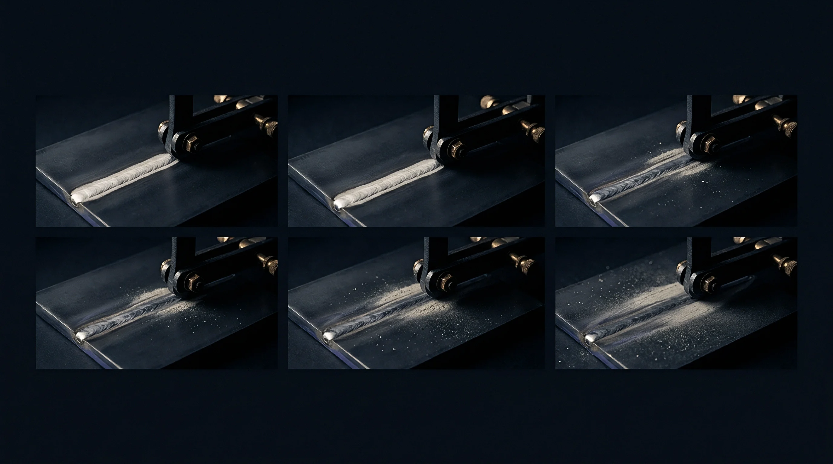
Cross-Shift Dosing Control in Plating Facilities
Shift handoffs represent structural vulnerabilities in plating line management. When operating responsibility transfers between engineers, unrecorded adjustments or delayed analytical samples trigger dosing errors. Standardized handoff logbooks enforce explicit logging of amp-hours run, chemical volumes added, filter exchange timestamps, and calibration checks.
Skipping a scheduled dopant replenishment near the end of a shift causes quiet chemical depletion, leaving the next shift operating with bath chemistry that yields panels vulnerable to void formation.
Filtration maintenance directly governs chemical stability. Activated carbon filter cartridges saturate over time, losing capacity to absorb organic breakdown products. Once saturated, organic impurities recirculate into the plating cell and embed sulfur and carbon into the copper film.
Establishing a forced filter exchange schedule based on amp-hours processed ~ rather than pressure drop across the filter housing ~ prevents organic contamination spikes.
Replacing thirty thousand dollars worth of micro-alloyed copper anodes after a supplier introduced uncertified recycled scrap demonstrated the necessity of raw material origin verification.


Fracture
Micro-void coalescence manifests as brittle interfacial fracture during mechanical stress testing. Solder joints formed on un-optimized copper deposits show adequate shear strength immediately after reflow. After thermal aging, however, accumulated Kirkendall voids create a continuous plane of weakness along the epsilon phase intermetallic boundary.
Under mechanical shock, drop testing, or ball shear testing, joints fracture along this void plane at loads far below design limits, producing the smooth, featureless fracture surface typical of complete brittle failure.
Optimizing dopant levels shifts the failure mode from brittle interfacial separation to ductile fracture in the bulk solder. When bismuth and nickel suppress void nucleation, the intermetallic interface holds under shear stress, forcing plastic deformation into the softer bulk solder alloy. Energy is absorbed and catastrophic detachment is avoided.
Residual ductile solder covering more than 85 percent of the sheared pad area confirms an interface free from continuous micro-void planes.
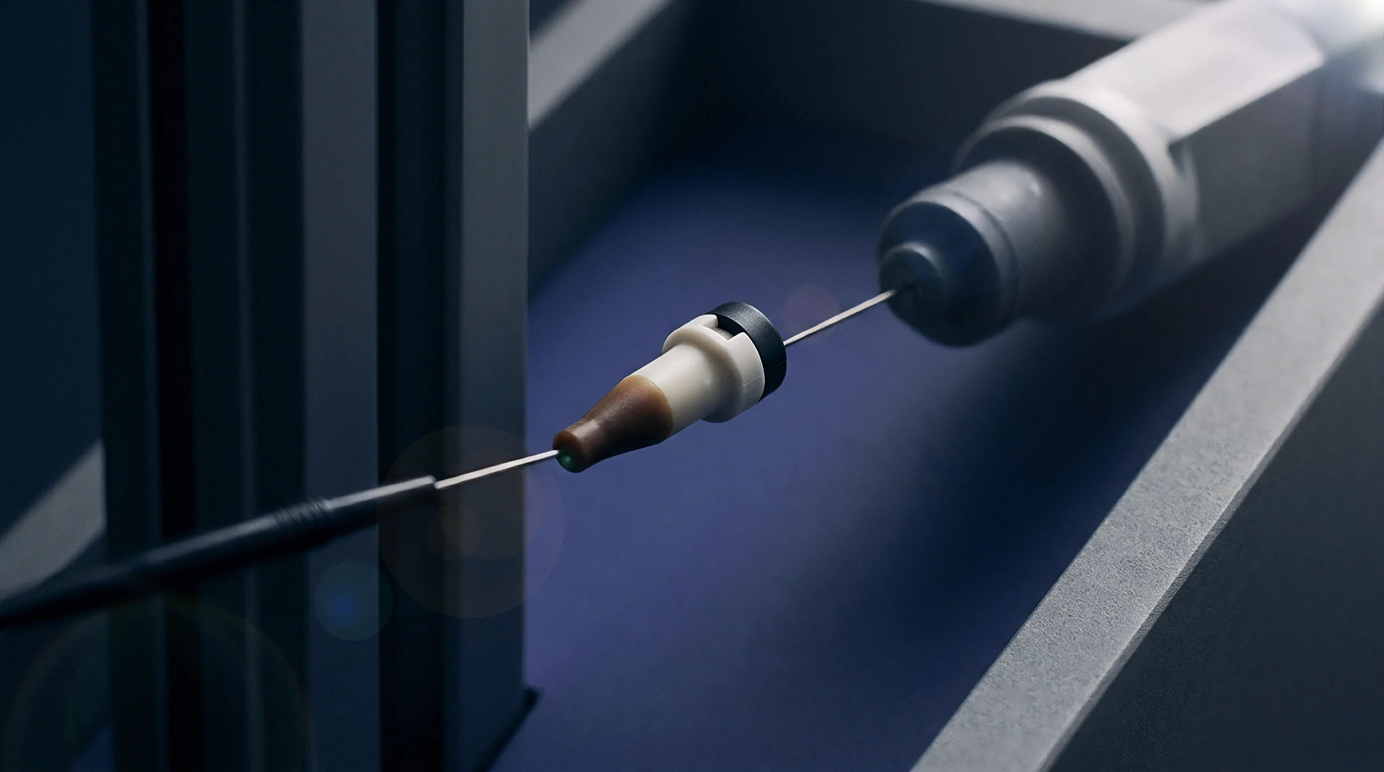
Post-Aging Ball Shear Failure Modes
High-speed ball shear testing quantifies mechanical integrity under controlled rates. Shear tools apply lateral force to solder spheres at speeds from 10 to 1000 millimeters per second. Testing post-reflow samples establishes baseline shear strength; re-testing identical lots after 500 hours of aging at 150 degrees Celsius exposes thermal degradation.
Un-passivated copper substrates typically lose 50 to 70 percent of their shear strength post-aging, shifting entirely from ductile to brittle failure.
| Dopant Condition | Aging Duration (Hours at 150C) | Mean Shear Force (Grams) | Ductile Mode Fraction (%) | Brittle Mode Fraction (%) |
|---|---|---|---|---|
| Undoped Pure Cu | 0 (As Reflowed) | 420 | 98.0 | 2.0 |
| Undoped Pure Cu | 500 | 165 | 12.0 | 88.0 |
| 25 PPM Bi Doped | 500 | 385 | 91.5 | 8.5 |
| 250 PPM Ni Doped | 500 | 360 | 88.0 | 12.0 |
| 25 PPM Bi / 250 PPM Ni | 500 | 410 | 96.5 | 3.5 |
Evaluating shear force data requires correlating peak force values with visual failure mode classification. A high shear force value paired with brittle fracture indicates latent stress concentration vulnerable to cyclic fatigue. A single rejected substrate lot incurred a scrap cost of 42,000 dollars after thermal aging revealed brittle interface separation.
True mechanical reliability requires both high peak shear force and a dominant ductile failure mode across tested joints.

Structural Analysis of Interface Separation
Scanning electron microscopy of fracture surfaces clarifies the mechanism of joint separation. Brittle fracture surfaces on undoped copper display micro-dimples corresponding to individual Kirkendall voids that coalesced before failure. These void dimples act as stress risers that initiate cracks and propagate under impact.
By contrast, dopant-optimized substrates show rough, torn surfaces where cracking occurred entirely within the bulk tin-silver-copper solder, leaving the underlying intermetallic layer unexposed.
Substrate supply contracts must incorporate explicit chemistry compliance requirements to enforce dopant optimization. To guarantee material traceability, suppliers must include the following analytical parameters in every plating batch certification dossier:
- Inductively Coupled Plasma Assay Results detailing exact deposit concentration values in parts per million for bismuth, nickel, and phosphorus.
- Organic Carbon Content Analysis verifying total carbon inclusion remains below 50 parts per million within the electroplated copper film.
- Thermal Aging Shear Test Certification demonstrating greater than 90 percent ductile failure modes after 500 hours at 150 degrees Celsius.
- Intermetallic Layer Thickness Records confirming epsilon phase growth stays below 2.5 micrometers following qualification bake routines.
Under Section 8.4 of the standard master supply covenant, failure to submit complete chemical assay dossiers with each shipment authorizes the buyer to hold payment without incurring late-payment interest penalties.


Yield
Controlling dopant chemistry directly dictates landed yield economics and cross-border commercial risk. Substrate processing represents a major fraction of total package value in advanced microelectronic assemblies. When micro-void coalescence causes field failures or reliability test rejections, financial losses far exceed the cost of the raw substrate panel.
Scrapping fully assembled, high-value die products due to substrate-level voiding destroys operating margins and triggers complex commercial disputes between buyers, assembly houses, and plating vendors.
Quantifying financial risk requires comparing total landed scrap costs against the operational expense of chemical control. Implementing automated ICP-OES monitoring and micro-alloying dopant delivery adds roughly 0.04 dollars per panel to substrate plating costs. By comparison, a single field recall of automotive control modules caused by interfacial joint failure carries costs exceeding hundreds of thousands of dollars in warranty claims, sorting, and arbitration.
The financial return on precise chemical control is immediate.

Landed Scrap Allocation and Rework Commercials
Commercial agreements between buyers and packaging suppliers must define financial responsibility for chemical defects discovered downstream. Standard manufacturing contracts often attempt to limit supplier liability to the bare replacement cost of unassembled substrate panels, leaving the buyer exposed to lost silicon die, mold compound, and assembly labor when defects surface during post-packaging qualification. Bath maintenance schedules should be written directly into the quality agreement attached to the purchase order.
Establishing clear commercial rules requires establishing structured batch disposition procedures upon detecting chemistry deviations. When quality audits reveal out-of-spec dopant levels, engineers evaluate batch risk using a strict decision framework:
- Quarantine all substrate panels produced during the operational window between the last compliant chemical assay and the non-compliant reading.
- Extract twenty representative coupons across five panels for accelerated 250-hour high-temperature storage life testing.
- Perform focused ion beam cross-sectioning to measure void area fractions along the intermetallic interface.
- Execute high-speed ball shear testing on aged samples to determine ductile-to-brittle failure ratios.
- Reject the entire quarantined lot for scrap if void area fraction exceeds 3.5 percent or brittle fracture mode exceeds 10 percent.
- Authorize conditional release for non-critical applications if void area fraction remains below 2.0 percent with zero brittle fracture modes detected.

Scrap Penalty Mechanics in Volume Supply Agreements
Enforcing quality compliance across international borders requires incorporating explicit financial penalties into supply agreements. Standard scrap penalty clauses mandate that if a plating lot fails thermal aging verification due to micro-void coalescence, the supplier absorbs the full cost of discarded component materials attached to defective substrates. This accountability aligns supplier incentives with floor-level chemical discipline, ensuring plating technicians do not sacrifice bath maintenance for throughput.
Suppliers operating under volume contracts frequently push to relax dopant monitoring during peak production periods to maximize panel output. Negotiating firm quality gates prevents throughput demands from eroding chemical oversight. Mandatory batch release sign-offs tied to verified ICP-OES dopant assays create an administrative barrier against shipping unverified product.
Establishing these commercial mechanisms protects cross-border operations from hidden process degradation, securing high-reliability interconnect performance across volume manufacturing runs.