Meaning
Acoustic imaging method utilizes high frequency sound waves to detect internal delamination or voids within the encapsulated layers of semiconductor devices. Application of scanning acoustic microscopy allows quality control engineers to inspect the internal structure of a package without having to cut it open or destroy it. This technique governs the verification of the bond between the silicon die and the lead frame and the integrity of the plastic molding compound.
It is practiced in failure analysis labs across China to identify the root causes of component malfunctions. The boundary of the method is limited to the detection of physical gaps or density changes and cannot identify purely electrical faults within the circuitry. It stops providing useful data when the materials are so thick or so porous that the sound waves are completely absorbed before they can return to the sensor.
Delamination Detection
Separation of internal layers within an electronic package is a common failure mode that can lead to catastrophic electrical shorts or open circuits. Scanning acoustic microscopy is particularly effective at identifying these separations because sound waves are reflected almost perfectly by even the thinnest layer of air. When the ultrasound beam hits a gap between the silicon die and the epoxy underfill, it produces a bright signal that is easily identified by the operator.
This is a critical step in the qualification of new packaging materials and in the monitoring of the assembly process. In the semiconductor manufacturing facilities of the Yangtze River Delta, this tool is used to ensure that the bonding process is consistent across every batch of chips. Early detection of delamination prevents the shipment of units that would likely fail soon after being placed into service.
Ultrasound Imaging
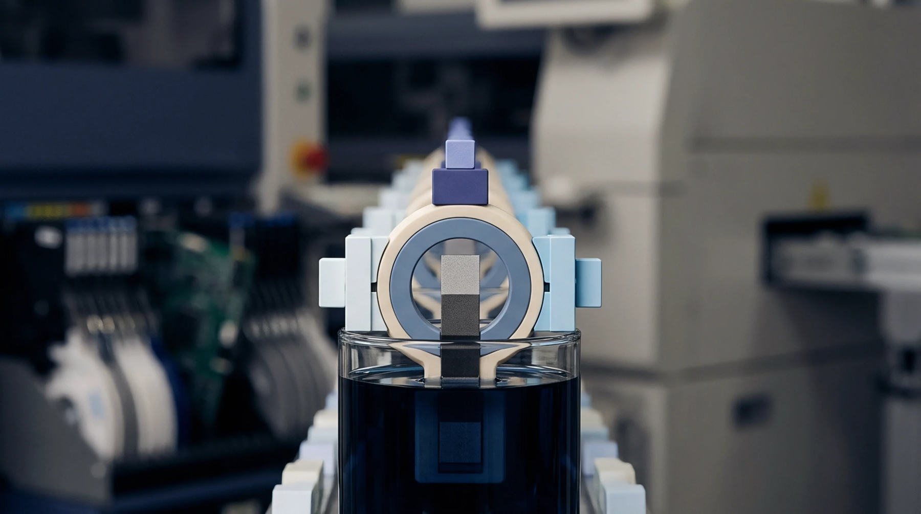
Translation of sound reflections into a visual map of the internal structure provides a detailed view of the component’s health. The scanning acoustic microscopy system moves a transducer across the surface of the part while it is submerged in a coupling fluid, usually deionized water. The transducer sends out a pulse of high frequency sound and then listens for the echoes that bounce back from the various internal interfaces.
The time it takes for the echo to return tells the system the depth of the interface, while the strength of the echo reveals the nature of the material. By processing these signals, the computer creates a high resolution image that shows every void and crack inside the package. This non-destructive view is essential for analyzing parts that have failed during environmental stress screening or during field operation.
Internal Inspection
Assessment of the overall quality of a batch of components depends on the ability to see what is happening beneath the surface. Scanning acoustic microscopy provides the data needed to make informed decisions about the reliability of a production run. If a specific type of void is found in a large number of samples, it indicates a systemic problem with the injection molding or the curing process.
Quality managers use this information to adjust the machine settings and to improve the yield of the factory. The tool is also used for counterfeit detection, as it can reveal if a chip has been re-packaged or if the internal structure does not match the original manufacturer’s specifications. This capability is vital for maintaining the security of the supply chain in the global electronics market.
The resulting images serve as a permanent record of the component’s internal integrity at the time of manufacture.