Establishing Commercial Warranty Liabilities for Latent Thermal Degradation in High Reliability Solder Joints
Latent thermal joint liabilities rely on defining contractual intermetallic thickness and void area limits backed by real-time reflow profiling records.


Shear
Thermal expansion mismatches between silicon packages, circuit board substrates, and lead-free solder alloys cause continuous cyclic displacement across printed circuit board assemblies. Operating high-reliability electronics in hot environments concentrates these mechanical micro-displacements right inside the solder joints. The resulting cumulative failure process remains completely invisible during initial factory functional testing, automated optical inspection, and short environmental stress screening.
Surface mount components on high-density circuit boards depend on solder joints for both electrical continuity and physical retention. Common lead-free alloys, mostly tin-silver-copper compositions like SAC305, respond in specific mechanical ways to cyclic temperature changes. The thermal expansion coefficient for an FR4 glass-reinforced epoxy substrate usually sits between 14 and 17 parts per million per degree Celsius along its planar axes.
Ceramic chip carriers and silicon dies, on the other hand, expand at only 2.5 to 6 parts per million per degree Celsius. In environments that swing from sub-zero temperatures up to 125 degrees Celsius, the board and the component body expand and contract at sharply different rates.
Factories frequently attribute thermal joint degradation to field vibration rather than inadequate intermetallic growth control during surface mount assembly.
Every thermal excursion forces stress across the interconnect matrix. Even at room temperature, solder sits at a high homologous temperature ~ the ratio of operating temperature to absolute melting point in Kelvin. For SAC305, melting around 217 degrees Celsius, operating at an ambient 85 degrees Celsius puts the alloy above 70 percent of its melting point.
At these temperatures, solder stops behaving as a pure elastic solid and instead undergoes rapid microstructural relaxation, plastic deformation, and steady mechanical drift under load.
Failure develops along predictable paths inside the solder volume. Stress builds first at the outer corners of surface-mount components, especially on large ball grid array packages and leadless chip carriers. As thermal cycling continues, micro-voiding and local grain restructuring seed tiny cracks that merge across the joint plane over thousands of operating hours.
Electrical conductivity often persists through simple mechanical contact until the crack severs the path entirely, triggering intermittent signal dropouts or complete open circuits.
- Micro-voiding coalescing at interfaces driven by continuous vacancy accumulation along the copper solder interface under high current density and thermal stress.
- Recrystallization along stress planes where localized plastic strain reorganizes the grain structure into coarse, low-angle boundaries susceptible to intergranular cracking.
- Intermetallic layer brittle fracture occurring at the narrow band between the tin-rich solder bulk and the underlying circuit board copper pad.
- Phase coarsening in tin-rich matrices where sub-micron Ag3Sn intermetallic particles migrate and grow, losing their ability to pin dislocation movement within the matrix.
Microstructural analysis of high-reliability power modules returned from industrial field deployments shows that joint degradation occurs predominantly within the narrow boundary layer right next to the intermetallic compound phase. Maintaining physical joint integrity relies on keeping a ductile grain matrix that can absorb displacement. Commercial disputes frequently arise because standard post-assembly testing fails to detect the early stages of this microstructural strain.
Field failures occurring past twelve months are frequently attributed to operational abuse outside specified thermal limits rather than baseline SMT thermal history.


Aging
Microstructural changes inside lead-free solder interconnects continue throughout the operational lifespan of an electronic assembly. Solid-state diffusion between the tin-rich solder alloy and the underlying copper contact pad drives ongoing growth of intermetallic compound layers. This chemical transformation alters the interface’s mechanical properties, replacing ductile solder alloy with hard, brittle intermetallic phases that offer poor resistance to mechanical shock and cyclic thermal displacement.

How Do Substrate Mismatches Accelerate Intermetallic Phase Changes?
Thermal energy drives atomic movement across the metallurgical junction between circuit board metallization and solder bulk. During initial reflow, molten solder dissolves copper from the board pad, forming a primary layer of Cu6Sn5 intermetallic compound, known as the eta phase. Once the assembly cools and goes into service, sustained high temperatures keep solid-state diffusion going.
Copper atoms migrate from the substrate pad into the Cu6Sn5 layer while tin atoms diffuse inward, converting the interfacial region into a secondary, copper-rich phase known as Cu3Sn, or the epsilon phase.
The growth rate of these intermetallic compound layers follows an Arrhenius relationship governed by temperature and activation energy, with total thickness increasing in proportion to the square root of time under heat exposure. The Cu3Sn phase has a higher lattice defect density and lower fracture toughness than the surrounding solder alloy. Once the Cu3Sn layer grows beyond a critical threshold of one to two microns, the joint becomes highly sensitive to mechanical strain.
| Solder Alloy Composition | IMC Growth Rate (nm/hr at 125°C) | Kirkendall Void Onset (Hours at 125°C) | Primary Microstructural Degradation Mode | Relative Fatigue Endurance Index |
|---|---|---|---|---|
| SAC305 (Sn96.5Ag3.0Cu0.5) | 1.85 | 750 | Kirkendall voiding at Cu3Sn/Cu interface and Ag3Sn coarsening | 1.00 |
| Innolot (Sn3.8Ag0.7Cu3.0Sb1.4Ni0.2Bi) | 0.92 | 2100 | Solid solution hardening maintains fine grain boundaries | 2.35 |
| Sn63Pb37 (Baseline Eutectic) | 2.40 | N/A (No Kirkendall) | Superplastic phase separation into large Sn and Pb rich domains | 0.65 |
| SAC105 (Sn98.5Ag1.0Cu0.5) | 2.10 | 600 | Rapid beta-Sn grain coarsening and intergranular cracking | 0.72 |
Solid State Intermetallic Compound Kinetics
Diffusion rates differ substantially between copper and tin atoms moving through the intermetallic crystal lattice. Copper diffuses into the Cu3Sn layer significantly faster than tin diffuses outward toward the solder bulk. This imbalanced flux leaves physical vacancies in the crystal structure on the copper side of the interface ~ a phenomenon known as Kirkendall voiding.
Over long operating periods at temperatures exceeding 100 degrees Celsius, these vacancies aggregate into microscopic voids along the interface between the copper pad and the Cu3Sn layer.
Void nucleation severely degrades the mechanical shear strength of the joint. Under cyclic thermal expansion, stress concentrates directly across this void-dense plane. The load-bearing area of the interface drops in direct proportion to the area fraction of accumulated Kirkendall voids.
Failure under these conditions occurs through rapid, brittle planar fracture along the void sheet, requiring minimal external energy once micro-cracks initiate.
When reflow dwell temperatures stay near liquidus for extended periods, microstructural grain growth outpaces stress relief and guarantees premature fatigue failures.

Kirkendall Void Nucleation under Sustained Thermal Dwell
Grain coarsening within the bulk solder alloy accompanies interfacial intermetallic growth. Newly solidified SAC305 solder contains tiny, highly dispersed silver-tin particles (Ag3Sn) embedded within a matrix of tin crystals. These fine particles restrict dislocation movement, giving mechanical strength to the bulk joint.
Sustained thermal exposure provides the activation energy needed for silver and tin atoms to diffuse across grain boundaries; smaller Ag3Sn particles dissolve into solution while larger precipitates grow thicker and move farther apart.
The solder matrix softens as particle spacing expands, losing its yield strength and resistance to creep deformation. Cyclic displacement from thermal expansion mismatches stops distributing evenly across millions of microscopic grain boundaries and begins concentrating along localized high-angle slip bands. This shift accelerates strain localization, driving the joint into rapid failure long before standard empirical fatigue models predict.
Thick intermetallic layers formed during initial reflow always crack before thin, fine-grained intermetallic structures under cyclic thermal stress.


Chamber
Environmental qualification testing validates electronic assembly durability by accelerating physical degradation in controlled test chambers. Establishing commercial warranty liability requires separating normal wear-out life from premature degradation caused by assembly line defects. Accelerated thermal cycling protocols expose assemblies to aggressive temperature extremes, forcing latent microstructural flaws into measurable electrical faults within practical test windows.

Accelerated Environmental Testing and Failure Isolation
Qualification routines rely on industry test standards like IPC-9701A and JESD22-A104. Profile selection directly determines which failure modes are induced during testing. Profiles typically swing between minus 40 degrees Celsius and 125 degrees Celsius at ramp rates between 10 and 15 degrees Celsius per minute.
Fast ramp rates create substantial dynamic temperature gradients across component bodies, adding transient thermal stress on top of steady-state expansion mismatches.
Dwell duration at maximum temperature determines how much creep strain relaxation and intermetallic growth occur per cycle. Dwells under ten minutes prevent the solder matrix from fully relaxing stress, causing tests to underestimate field creep damage. Extending dwell times to thirty or forty-five minutes allows complete relaxation, converting elastic strain into plastic deformation and accelerating Kirkendall void formation.
Under 125 degrees Celsius continuous dwell, intermetallic compound growth rates at the copper-solder interface double every 800 thermal hours in SAC305 joints.
Arrhenius acceleration factors translate chamber performance into field reliability projections. Industrial power electronics operating at a continuous ambient temperature of 60 degrees Celsius show an acceleration factor of roughly 12.5 when subjected to a 125 degrees Celsius test chamber, assuming an activation energy of 0.68 electron volts for SAC305 intermetallic growth. Lower activation energies around 0.50 electron volts yield acceleration factors closer to 5.2.
Because small shifts in assumed activation energy alter projected field survival by several years, defining explicit activation energy values in supply contracts is essential.
- Dwell time verification at thermal extremes ensuring complete thermal equilibrium across massive components before initiating ramp phases.
- Continuous resistance monitoring during cycling using high-speed event detectors capable of capturing microsecond intermittent open circuits.
- Metallographic cross sectioning post dwell to quantify intermetallic growth thickness and Kirkendall void planar density.
- Acoustic scanning for delamination detection mapping physical separation at component interfaces without destructive sectioning.
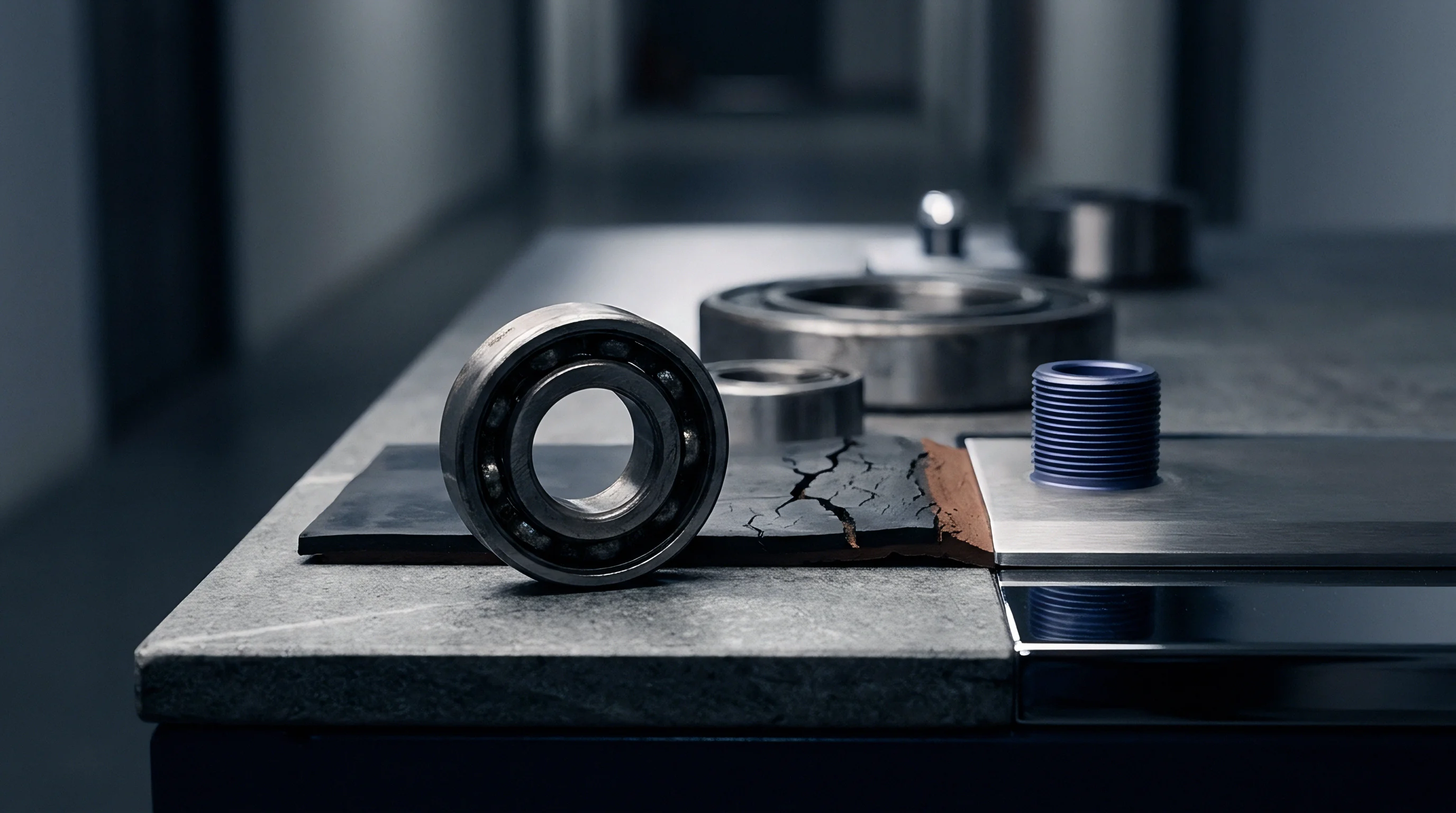
Non Destructive Inspection and Cross Sectional Metallography
Destructive metallurgical cross-sectioning remains the definitive method for establishing root causes in latent solder failure. Technicians cold-mount sectioned components in epoxy resin, then grind and polish the surface to a 0.05-micron colloidal silica finish. Etching the polished surface with an ammonium persulfate reagent reveals grain boundaries, intermetallic phase distributions, and micro-cracks under scanning electron microscopy.
Quantitative image analysis measures total intermetallic layer thickness and calculates the area fraction of Kirkendall voids along the interface. Void area fractions above fifteen percent along the Cu3Sn interface point to severe thermal degradation caused by excessive reflow heat or defective substrate plating chemistry. Scanning acoustic microscopy offers a non-destructive alternative, using high-frequency ultrasound to map planar cracks and void sheets across entire ball grid arrays before cutting.
Engineers remain divided over whether high-frequency thermal shock profiles adequately replicate decades of low-amplitude daily thermal cycling in field-deployed power electronics.


Allocation
Commercial contracts governing high-reliability electronic assemblies must bridge technical failure modes and financial risk distribution. Latent thermal solder degradation presents a unique legal challenge because assemblies pass initial factory acceptance tests without flaw. Warranty structures must precisely define the technical criteria that convert a field failure into a vendor-indemnified event, separating manufacturing defects from operational abuse in the field.

Contractual Classification of Latent Interconnect Defects
Supply agreements divide risk between patent defects visible at delivery and latent defects that appear only after extended exposure. Thermal solder degradation falls squarely into the latent category. Contracts must set explicit technical thresholds to trigger vendor financial liability.
Standard two-year product warranties often expire before latent voiding causes failures, leaving buyers exposed to major replacement costs in years three through five.
Quality Assurance Agreements (QAAs) eliminate ambiguity by tying warranty coverage to microstructural performance standards rather than time windows. If a returned assembly shows intermetallic growth rates or Kirkendall void densities beyond baseline qualification specs, the defect is classified as a systemic manufacturing execution failure. This classification bypasses unit-by-unit replacement terms, unlocking batch-level recall remedies and full financial indemnification.
| Latent Failure Mechanism | Diagnostic Evidence Metric | Primary Fault Allocation | Contractual Remedy Trigger | Standard Liability Limit |
|---|---|---|---|---|
| Excessive IMC growth from reflow overheat | Total IMC thickness exceeding 4.5 µm at delivery | Assembly Contractor (EMS) | Batch failure rate exceeding 0.5% of total lot | 100% of lot replacement cost plus reverse logistics |
| Kirkendall voiding from pad contamination | Interfacial void area fraction exceeding 12% | Bare Board Supplier / EMS | Single failure confirmed by metallurgical audit | Full component cost and field service reimbursement |
| CTE mismatch crack from unapproved substrate | Glass transition temperature (Tg) below spec | Material Supplier / EMS | Engineering revision verification mismatch | Tooling redesign cost plus scrapped inventory balance |
| Thermal fatigue from field over-temperature | Logged thermal profiles exceeding MSA limit | Original Equipment Manufacturer (OEM) | Telemetry log proof of thermal boundary breach | Zero vendor liability; buyer absorbs field loss |

Boundary Conditions and Operating Envelope Mapping
Defining the legal operating envelope requires documenting real field mission profiles against design specifications in contract schedules. Component suppliers and contract manufacturers limit exposure by specifying maximum continuous operating temperatures, peak thermal ramp rates, and maximum allowable thermal cycles over the product lifecycle. These parameter envelopes are attached as binding exhibits to the Master Supply Agreement (MSA).
Field telemetry and onboard environmental logs provide crucial evidence during warranty adjudication. Modern high-reliability assemblies frequently include environmental logging microcontrollers or micro-thermal sensors. When field failures occur, logged data proves whether operating conditions stayed within contractual bounds.
If environmental logs show compliance with agreed limits while solder joints exhibit premature micro-cracking, legal presumption of fault shifts entirely to the contract manufacturer.
- Explicit thermal mission envelope parameters defining maximum ambient temperatures, cycle frequencies, and lifetime thermal shock counts.
- Batch failure threshold criteria establishing the exact failure percentage within a manufacturing lot that triggers full lot rejection and financial recovery.
- Root cause adjudication procedures naming independent metallurgical laboratories tasked with executing binding failure analysis.
- Financial caps and direct damage formulas defining recoverable expenses including de-installation, direct freight, bench diagnostics, and replacement assembly costs.
Tiered financial recovery models establish clear warranty indemnification terms in commercial contracts. A typical framework sets specific recovery values based on failure timing: 100 percent vendor reimbursement for failures within 10,000 operating hours where intermetallic thickness exceeds 3.5 microns, scaling down to 50 percent reimbursement up to 25,000 operating hours. Tying financial recovery directly to measured metallurgical metrics eliminates subjective disputes over field environmental severity.
Section 18.4 of the refined Quality Assurance Agreement shifts full recall costs to the manufacturer whenever joint cross-sectional voiding exceeds eight percent within thirty-six months of delivery.


Audit
Preventing latent thermal joint failures requires physical verification of production variables inside contract manufacturing plants. SMT reflow profiling governs initial intermetallic layer formation. Line operators frequently optimize profiles for visual appearance and minimal bridging defects, unintentionally creating thermal conditions that degrade long-term durability through excessive heat exposure or insufficient cooling rates.

Reflow Oven Thermal Profiling and Microstructure Control
Surface mount assembly lines running high-reliability lead-free production require continuous multi-channel thermal profiling. Ovens with ten to twelve heating zones provide the thermal control needed to maintain optimal liquidus parameters. Time Above Liquidus (TAL) for SAC305 alloy must be tightly managed between 45 and 75 seconds, with peak temperatures kept between 235 and 245 degrees Celsius.
Exceeding 90 seconds TAL or a 250 degrees Celsius peak reflow dramatically increases initial Cu6Sn5 intermetallic thickness, accelerating aging degradation down the line.
Nitrogen atmosphere control within the reflow chamber limits surface oxidation during soldering. Oxygen concentrations must stay below 500 parts per million, with high-reliability automotive lines targeting levels below 100 parts per million. Low-oxygen environments reduce solder paste flux breakdown, improving wetting and reducing microscopic flux void entrapment within the joint volume.
Lower voiding directly correlates with improved fatigue life under cyclic thermal loading.
| Process Parameter | Nominal Control Target | Latent Failure Risk from Deviation | Real Time Monitoring Infrastructure | Floor Verification Cadence |
|---|---|---|---|---|
| Time Above Liquidus (TAL) | 45 – 75 seconds | Excessive initial intermetallic thickness (>2.5 µm) | Continuous profiler pass-through tracking | Every 12 operating hours |
| Reflow Cooling Zone Ramp Rate | -3.0 to -5.0 °C/sec | Coarse grain formation and low creep resistance | Integrated thermocouple array readouts | Continuous automated logging |
| Nitrogen Chamber O2 Level | < 200 ppm | Interfacial oxide entrapment and micro-voiding | Continuous electrochemical sensor log | Per shift manual calibration check |
| Solder Paste Thaw Dwell | 4 hours room temp | Moisture absorption causing explosive reflow voiding | Barcode time-stamp tracking system | 100% of used paste jars |

Traceability Infrastructure and Process Parameter Logs
Cooling rates after reflow govern initial grain size in the solidified solder matrix. Rapid cooling between 3 and 5 degrees Celsius per minute forces tin and silver to solidify into fine, highly dispersed phases. Cooling slower than 2 degrees Celsius per minute allows silver-tin intermetallic compounds to precipitate into large, coarse plates that concentrate stress and lower fatigue resistance.
Plant audits verify that cooling zone heat exchangers operate cleanly and fan speed settings remain locked against unauthorized line adjustments.
Audit procedures enforce total lot traceability from raw component receiving through final packaging. Modern manufacturing execution systems (MES) bind specific reel lot numbers of solder paste, component date codes, board fabrication lots, and real-time reflow profile logs to individual board serial numbers. When field returns show latent thermal failure characteristics, these logs allow quality engineers to isolate exact production dates, SMT lines, and serial number bands, preventing unnecessary recalls of conforming product lots.
- Inspect the SMT line reflow oven log history for zone temperature deviations exceeding two degrees Celsius.
- Verify nitrogen atmosphere analyzer calibration records to confirm oxygen displacement stays under 400 parts per million.
- Pull five raw printed circuit board assemblies from the SMT output conveyor for immediate X-ray void inspection.
- Compare solder paste lot numbers against warehouse storage refrigeration logs and thaw duration stamps.
- Cross reference automated X-ray void measurements against the contractual five percent surface area threshold.
Baseline field failure rates attributable purely to latent intermetallic thermal creep in ten-year outdoor automotive applications hover between 120 and 450 parts per million. Estimating this range precisely is difficult because field returns combine thermal cycling strain with vibration and ambient moisture. Buyers manage this statistical uncertainty by negotiating a fixed 300 parts per million baseline non-action allowance into the supply contract, establishing clear financial liability boundaries before initiating formal lot disputes.
Unannounced process shifts, such as reducing reflow cooling fan speeds to cut facility power costs, directly alter microstructural solidification and induce premature field failures.

Reserve
Financial accounting standards require electronics manufacturers to establish balance sheet reserves for prospective warranty liabilities. Latent thermal solder joint failures present a complex calculation due to their delayed manifestation window. Provisions based solely on early return data significantly underestimate true field exposures, leaving businesses vulnerable to severe earnings adjustments when aging field units reach their thermal wear-out threshold.

Financial Provisioning and Latent Defect Escrow Holdbacks
Actuarial modeling of latent warranty obligations uses Weibull distribution calculations to project failure probabilities over extended time horizons. Early-life infant mortality yields a Weibull shape parameter beta below 1.0, while random mid-life failures sit near a beta of 1.0. Latent thermal joint degradation, driven by accumulative wear-out kinetics, shows a steep Weibull shape parameter between 2.5 and 4.2.
Failure rates remain negligible during initial operating months, then escalate rapidly as the population approaches its characteristic life threshold.
Financial holdbacks and escrow structures safeguard buyers against supplier insolvency during long latent failure windows. Contract terms routinely mandate holding back two to five percent of total purchase order value in an interest-bearing escrow account for thirty-six months post-delivery. Alternatively, suppliers provide irrevocable standby letters of credit issued by Tier 1 international financial institutions.
If metallurgical analysis confirms systemic latent thermal degradation in field units, the buyer draws directly on the escrow or letter of credit to cover field containment, customer notification, and unit replacement.
Arbitration Protocols and Independent Metallurgical Adjudication
Technical dispute resolution clauses govern the validation and execution of warranty claims. When high-value field failures occur, suppliers routinely contest liability by arguing that operating environments exceeded agreed thermal boundaries. Establishing an independent expert adjudication protocol within the supply agreement prevents drawn-out legal proceedings while maintaining clear procedural pathways for financial recovery.
Historical data from high-reliability military and subsea infrastructure electronics offers valuable lessons regarding microstructural intermetallic control. Early high-reliability deployments suffered unexpected field losses when undoped lead-free interconnects developed extensive micro-voiding and tin whisker growth during extended thermal dwell periods. Modern alloy doping techniques utilizing micro-additions of nickel, bismuth, and antimony were subsequently developed to stabilize grain boundaries and suppress vacancy aggregation under extreme environmental stresses.
Contractual settlement procedures stipulate that when field defect rates exceed agreed batch limits, an accredited independent metallurgical laboratory performs standardized cross-sectional analysis, energy-dispersive X-ray spectroscopy, and electron backscatter diffraction. Lab findings serve as binding evidence for financial allocation. If analytical results show mean intermetallic compound thickness exceeding 4.0 microns or Kirkendall void area ratios exceeding 10 percent on units operating within contractual timeframes, the supplier reimburses all diagnostic testing fees, waives dispute rights, and releases escrowed funds to cover full customer indemnification provisions.