Quantifying Long Term Thermo Mechanical Fatigue and Kirkendall Voiding in Lead Free Interconnects
Accelerated thermal cycling models coupled with intermetallic void area fraction measurements quantify fatigue life and prevent catastrophic field failures.

Creep
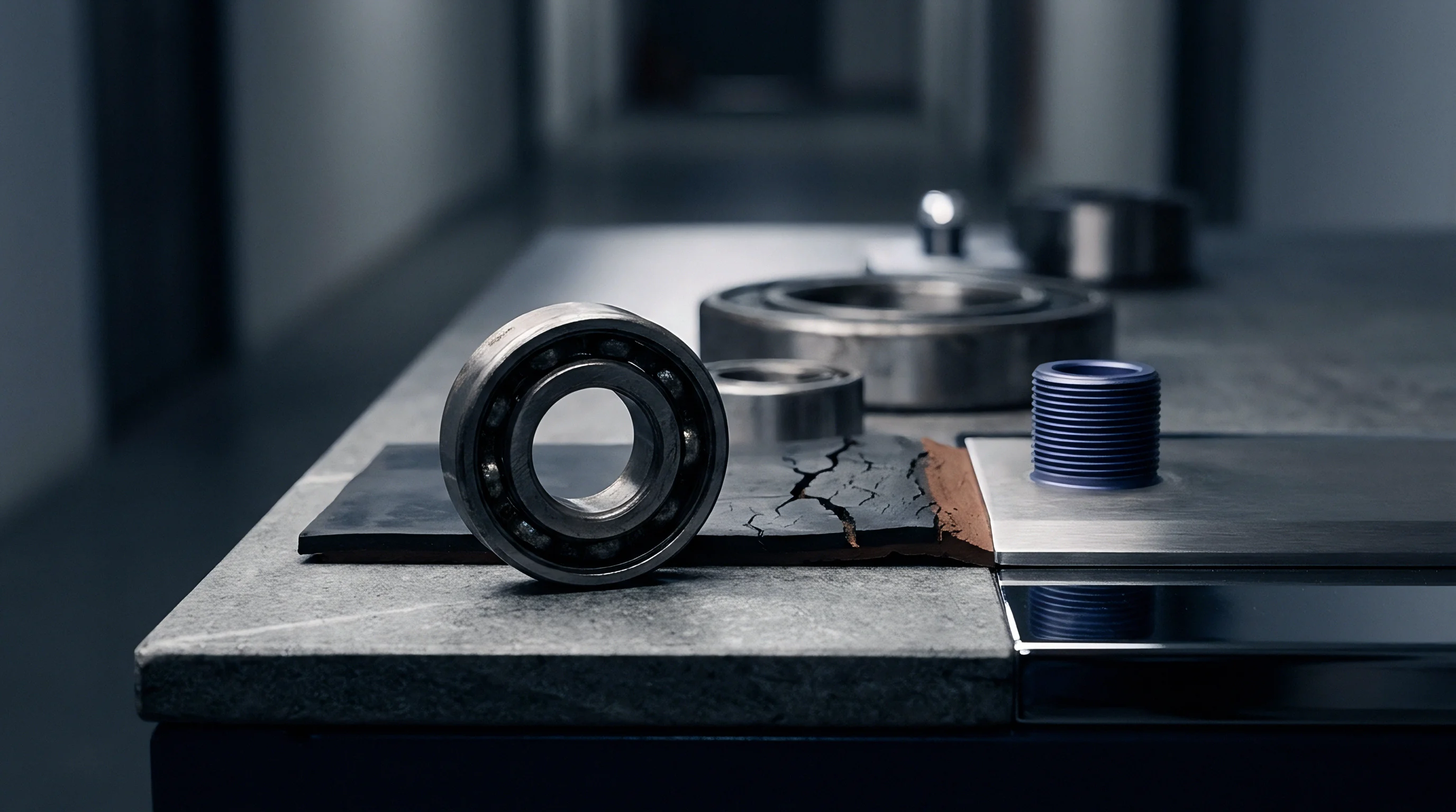
A polished metallurgical mount sits under the optical objective in a Dongguan failure analysis laboratory, displaying a forty-five-degree shear fracture across the outer corner ball of a fine-pitch ball grid array. The component endured fifteen hundred thermal cycles between minus forty degrees Celsius and one hundred twenty-five degrees Celsius. Plastic deformation concentrates entirely in the bulk tin matrix adjacent to the package interface pad, where cyclic shear strains reach three percent per thermal swing.
Thermal expansion mismatches govern strain. The silicon die expands at 2.6 parts per million per Kelvin, while the flame-retardant printed circuit board expands at 16 parts per million per Kelvin in the in-plane axes. This expansion differential forces the outermost solder interconnects to absorb cyclic displacement through time-dependent inelastic shear.
Near homologous temperatures of 0.65 to 0.85 Tm, lead-free alloys deform primarily through dislocation climb and grain boundary sliding. SAC305, composed of 96.5 percent tin, 3.0 percent silver, and 0.5 percent copper, exhibits high sensitivity to strain rate and operating temperature. Silver additions raise yield strength.
When ambient temperatures rise within an industrial enclosure, the flow stress of the solder joint drops sharply. The solder creeps. Dislocation networks pile up against intermetallic precipitates of Ag3Sn and Cu6Sn5 dispersed throughout the beta-tin grains.
Over prolonged dwell periods at elevated temperatures, stress relaxation converts elastic deformation into creep strain, depleting the fatigue margin of the physical interconnect.
SAC305 interconnects subjected to a forty-minute thermal dwell at one hundred twenty-five degrees Celsius lose over sixty percent of their initial shear resistance within five hundred thermal cycles.
Microstructural coarsening accelerates the accumulation of shear damage across subsequent temperature excursions. The sub-micron Ag3Sn spheroids, which initially pin grain boundaries and prevent grain dislocation motion, coalesce into coarse, widely separated particles under continuous thermal exposure. Thermal strain drives dislocation movement.
As these pinning precipitates coarsen, the alloy softens locally. Inelastic strain concentrates into bands across the primary shear plane of the solder sphere, creating microstructural channels where localized damage accumulates rapidly during subsequent hot dwells.
- Grain boundary sliding displaces adjacent tin crystals during elevated temperature dwell periods, initiating microcracks along high-angle boundaries.
- Intermetallic phase coarsening depletes solute atoms from the tin bulk, reducing precipitation hardening over extended thermal operational life.
- Localized recrystallization concentrates inelastic strain into narrow shear bands near the component package corner pads, and substantial plastic deformation occurs within these softened bands.
- Substrate pad warpage generates mixed-mode tensile and tearing stresses across the corner solder spheres during temperature swings.

Constitutive Modeling of Inelastic Solder Strain
Viscoplastic deformation dominates the mechanical response of SAC305 joints under alternating temperatures. The Garofalo hyperbolic sine creep equation provides an accurate description of the steady-state creep strain rate across varied stress regimes, bridging low-stress power-law climb and high-stress power-law breakdown. In this formulation, the steady-state strain rate depends on the applied shear stress, an empirical stress multiplier, a stress exponent typically measured between 4.2 and 5.5 for lead-free solders, and an activation energy aligned with self-diffusion in beta-tin, roughly 100 kilojoules per mole.
When an assembly experiences sustained dwell periods at eighty-five degrees Celsius or higher, steady-state creep accounts for more than eighty percent of total plastic deformation accrued per cycle.
Finite element analysts combine the Garofalo model with kinematic hardening laws to simulate the hysteresis loop of the corner interconnect under board-level thermal loading. The area enclosed by the shear stress versus shear strain hysteresis loop represents the accumulated inelastic strain energy density per thermal cycle. Cycling frequency alters fatigue life.
In high-density ball grid arrays, maximum strain localization develops within a twenty-micrometer zone directly beneath the package-side intermetallic compound boundary. Shear loads concentrate at corners. Crack initiation occurs within this narrow, highly strained zone once the cumulative plastic work density exceeds the characteristic fracture energy threshold of the alloy.

Anand Viscoplastic Parameters for SAC Alloys
Nine distinct material constants define the stress saturation and strain hardening response across fluctuating thermal environments. The Anand constitutive model treats plastic flow and strain hardening as unified viscoplastic processes, omitting an explicit yield criterion. The evolution equation governs an internal scalar state variable representing average resistance to plastic flow.
Parameters include the initial value of flow resistance, the activation energy divided by the universal gas constant, the pre-exponential factor, the stress sensitivity exponent, the strain rate sensitivity of hardening, and saturation coefficients that capture temperature-dependent dynamic recovery.
| Parameter | Symbol and Units | SAC305 | SAC405 | Sn63Pb37 |
|---|---|---|---|---|
| Initial flow resistance | s0 (MPa) | 1.30 | 2.20 | 12.41 |
| Activation energy term | Q / R (K) | 9,970 | 10,790 | 9,400 |
| Pre-exponential factor | A (s-1) | 1.79E7 | 3.50E7 | 4.00E6 |
| Multiplier of stress | ξ (dimensionless) | 0.35 | 0.40 | 1.50 |
| Strain rate sensitivity | m (dimensionless) | 0.25 | 0.22 | 0.30 |
| Hardening coefficient | h0 (MPa) | 1,800 | 2,400 | 1,379 |
| Coefficient for saturation | s_hat (MPa) | 30.2 | 38.5 | 40.0 |
| Strain rate sensitivity of saturation | n (dimensionless) | 0.012 | 0.015 | 0.070 |
| Temperature sensitivity of saturation | a (dimensionless) | 1.78 | 1.65 | 1.30 |
The parameter differences between SAC305 and SAC405 reflect the influence of silver content on dislocation immobilization. Higher silver fractions produce a denser dispersion of sub-micron Ag3Sn intermetallics, raising the saturation flow resistance and initial hardness. The alloy resists early cyclic creep.
Under aggressive thermal shock, however, the stiffer SAC405 matrix transfers greater mechanical shock loads directly into the brittle intermetallic interfaces at the substrate pad. The factory explains that corner joint cracking represents normal component settling that can be cured by extending the reflow cooling zone profile.
Diffusion
Atomic transport across the interface between copper pads and tin-based solders operates at asymmetrical rates. During soldering and subsequent solid-state aging, copper atoms dissolve into the molten solder to form copper-tin intermetallic compounds. Upon solidification, a layer of Cu6Sn5 forms immediately against the copper base.
Copper diffuses faster than tin. Elevated operating temperatures drive copper atoms out of the printed circuit board substrate pad and into the Cu6Sn5 lattice, converting the interface into a secondary, copper-rich intermetallic phase identified as Cu3Sn. Unbalanced fluxes generate vacant sites.
Excessive organic brighteners in the electrolytic copper plating bath produce rapid Kirkendall void coalescence under sustained thermal exposure.
In 1947, Ernest Kirkendall demonstrated that insoluble markers placed at a brass-copper interface shift position during high-temperature annealing because zinc atoms diffuse outward faster than copper atoms diffuse inward. This fundamental metallurgical displacement confirmed that atomic migration occurs via vacant lattice sites rather than direct atom-swapping mechanisms. In modern surface mount electronics, an identical phenomenon unfolds between the copper substrate pad and the solder joint.
Copper atoms possess higher mobility than tin atoms within the Cu3Sn intermetallic phase. Copper migrates rapidly toward the bulk solder to feed Cu6Sn5 growth, leaving an excess flux of vacancies behind in the Cu3Sn layer adjacent to the copper interface.

Where Do Vacancy Gradients Trigger Microvoid Coalescence?
The unequal flux of elemental species across the Cu3Sn intermetallic sublayer leaves unbalanced lattice sites. As copper leaves the pad surface faster than tin moves downward to occupy the vacated positions, vacancies supersaturate the lattice near the Cu3Sn and copper boundary. Vacancies migrate along grain boundaries and precipitate into discrete microvoids ranging from 50 nanometers to 300 nanometers in diameter.
Interfacial voids coalesce into microcracks. Once operating temperatures exceed eighty degrees Celsius, vacancy diffusion rates accelerate exponentially, transforming isolated nanoscale cavities into continuous planar void networks along the copper interface.
Electroplating bath chemistry dictates the density of vacancy nucleation sites. Standard printed circuit board fabrication utilizes acid copper plating baths containing organic levelers, carriers, and sulfur-bearing brighteners to ensure uniform copper deposition across blind microvias and through-holes. High concentrations of bis(3-sulfopropyl) disulfide or thiourea breakdown products co-deposit with the copper film, trapping sulfur, chlorine, and carbon impurities within the copper grain structure.
During thermal aging, these entrapped impurity atoms segregate to the Cu3Sn and copper interface, lowering the free energy barrier required for vacancy nucleation and dramatically increasing the volume fraction of microvoids.
Intermetallic Growth and Phase Transformations
High-temperature storage converts the initial scallop-shaped Cu6Sn5 layer into a planar bilayer structure containing Cu3Sn. The total thickness of the intermetallic bilayer grows parabolically with aging time, driven by bulk and grain-boundary diffusion. Cu6Sn5 forms during the liquid-solid reaction at reflow temperatures of two hundred forty degrees Celsius, but Cu3Sn requires thermal activation in the solid state, generally appearing after prolonged exposure above seventy-five degrees Celsius.
The interface develops distinct mechanical properties as the Cu3Sn phase thickens, because Cu3Sn exhibits lower fracture toughness than the adjacent Cu6Sn5 layer.
| Surface Finish Architecture | Initial IMC Composition | Aged IMC Layer (500h at 150°C) | Diffusion Barrier Performance | Kirkendall Susceptibility |
|---|---|---|---|---|
| Bare Electrolytic Copper | Cu6Sn5 (scallop) | Cu6Sn5 + Cu3Sn (bilayer) | Zero barrier; rapid Cu migration | High (sulfur co-deposition dependent) |
| Electroless Nickel Immersion Gold (ENIG) | (Ni,Cu)3Sn4 | (Ni,Cu)3Sn4 + Ni3P (crystallized) | Nickel restricts Cu; forms P-rich band | Negligible (replaced by black pad risk) |
| Electroless Nickel Electroless Palladium (ENEPIG) | (Pd,Ni)Sn4 + (Ni,Cu)3Sn4 | (Ni,Cu)3Sn4 (stable) | Dual barrier protects nickel layer | Extremely low interfacial cavitation |
| Immersion Silver over Copper | Cu6Sn5 (planar) | Cu6Sn5 + Cu3Sn (thickened) | Silver dissolves instantly into solder | Severe under sulfur-rich plating baths |
| Organic Solderability Preservative (OSP) | Cu6Sn5 (coarse scallop) | Cu6Sn5 + Cu3Sn (accelerated) | No metallic barrier layer present | Elevated with high-speed acid Cu baths |
The fracture resistance of the aged interconnect deteriorates sharply once the Cu3Sn layer exceeds a thickness of two micrometers. Brittle fracture follows cyclic stress. When an external shock or thermal-expansion shear stress strikes the joint, the crack path propagates through the compromised Cu3Sn layer rather than through the bulk solder.
Nickel barriers suppress voiding. Plating baths with sulfur contamination above twenty parts per million generate an order of magnitude more voiding than high-purity chemical baths. A clean copper interface with fine equiaxed grain structure and low impurity levels maintains shear strength throughout the functional life of the assembly.


Cycling
Accelerated thermal screening subjects electronic assemblies to programmed environmental swings to compress decades of field life into months. Environmental chambers enforce strict temperature ramps, upper dwells, and lower dwells to simulate daily operating conditions experienced in automotive engine compartments, aerospace avionics bays, or solar inverters. Chamber dwell times alter microstructure.
The choice of temperature limits, transition rates, and soak durations alters the active creep mechanisms within the lead-free solder joints, determining whether failure occurs via ductile fatigue propagation through the bulk alloy or via brittle fracture along the intermetallic boundary.
Standard qualification procedures rely on standardized profiles defined in IPC-9701 and JEDEC JESD22-A104. In an automotive under-hood validation, test units undergo cycles between minus forty degrees Celsius and one hundred twenty-five degrees Celsius or one hundred fifty degrees Celsius. Transition times of less than fifteen minutes generate severe thermal gradients across heavy components such as magnetic chokes and shielded power modules.
The joint separates cleanly. Rapid temperature swings induce transient out-of-plane warpage in thin printed circuit boards, imposing dynamic peel stresses on the outer rows of ball grid arrays while the alloy remains cold and brittle.
IPC-9701 thermal cycling test criteria reassign complete batch replacement costs to the component packager whenever electrical opens appear prior to one thousand cycles.
Dwell periods must provide sufficient duration for complete stress relaxation without inducing artificial metallurgical aging that never occurs in the field. At one hundred twenty-five degrees Celsius, SAC305 joints relax seventy percent of their accumulated thermal stress within ten minutes. Extending dwell times to sixty minutes yields only marginal additions to cyclic creep strain, while tripling total chamber occupancy time and operating expense.
Long high-temperature soaks promote excessive solid-state diffusion, artificially swelling the Cu3Sn layer and triggering Kirkendall cavitation that distorts lifetime predictions for moderate-temperature consumer applications.
- Baseline cross-section validation establishes initial intermetallic thickness and confirms zero pre-existing microvoids along copper boundaries prior to chamber loading; skipping this step invalidates subsequent crack attribution.
- In-situ resistance daisy-chain logging detects the exact cycle of electrical open circuits caused by thermo-mechanical fatigue, recording transient micro-cracking events that heal during chamber cooling.
- Periodic acoustic tomography extraction inspects component ball arrays at two-hundred-cycle intervals to monitor planar delamination before complete physical joint detachment occurs.
- Terminal metallurgical failure logging documents intermetallic fracture paths under electron microscopy; discovering brittle interfacial cleavage shifts replacement liabilities directly onto the substrate plating line.

Can Accelerated Thermal Profiles Predict Automotive Lifetimes?
Chamber dwell periods between minus forty degrees Celsius and one hundred twenty-five degrees Celsius induce creep damage in solder spheres. Engineers calculate acceleration factors to translate cycles to failure under laboratory conditions into predicted service years in the field. The modified Norris-Landzberg model adjusts the classical Coffin-Manson relation by incorporating cyclic frequency and maximum temperature corrections.
The acceleration factor equals the ratio of thermal fatigue cycles in the field to cycles in the test chamber, expressed as:
AF = (ΔTtest / ΔTfield)1.9 · (ffield / ftest)0.33 · exp((Ea / k) · (1 / Tmax,field – 1 / Tmax,test))
In this relationship, ΔT represents the temperature range of the cycle, f denotes the cycling frequency, Ea is the effective activation energy, k is the Boltzmann constant (8.617E-5 eV/K), and Tmax represents the peak absolute temperature reached during the cycle in Kelvin. For SAC305 interconnects, standard industry calculations apply an empirical activation energy of 0.12 electron-volts and a frequency exponent of 0.33. This standard activation energy figure rests on published test series analyzing plastic work accumulation across 256-pin plastic ball grid arrays cycled between 0°C and 100°C. If field operating environments involve sustained dwell periods exceeding four hours at ninety degrees Celsius, grain boundary sliding and matrix diffusion dominate, shifting the true physical activation energy toward 0.40 electron-volts and cutting the actual field life by more than half relative to the calculated projection.
| Test Condition | Temperature Range | Ramp Rate | Dwell Duration | Predominant Failure Mode |
|---|---|---|---|---|
| Condition A | -55°C to +85°C | 10°C / min | 10 minutes | Bulk solder fatigue crack propagation |
| Condition B | -40°C to +125°C | 15°C / min | 15 minutes | Mixed-mode bulk shear and IMC microcracking |
| Condition G | -40°C to +150°C | 15°C / min | 15 minutes | Interfacial cleavage across Cu3Sn layer |
| Condition J | 0°C to +100°C | 10°C / min | 10 minutes | Grain boundary recrystallization fatigue |
| Condition N | -40°C to +85°C | 12°C / min | 20 minutes | Slow ductile striation growth in beta-tin |
Discrepancies arise when testing under Condition G because peak temperatures of one hundred fifty degrees Celsius exceed the thermal stability limit of many organic package substrates. Substrates soften near their glass transition temperatures, artificially reducing in-plane expansion mismatches and underestimating fatigue damage. Concurrently, vacancy diffusion rates surge at one hundred fifty degrees Celsius, generating massive Kirkendall voiding that would require thirty years to develop at normal operational temperatures of fifty degrees Celsius.
Conditioning regimes must avoid driving the physical hardware across metallurgical phase boundaries that remain uncrossed during regular field service.

Coffin Manson and Energy Partitioning Formulations
Empirical fatigue relationships relate plastic shear range directly to the mean repetitions preceding interconnect fracture. The plastic strain range accounts for the irreversible plastic and creep deformation experienced by the solder joint during each thermal swing. The Coffin-Manson relation expresses fatigue life as Nf = C · (Δγp)-c, where Nf represents cycles to crack initiation, Δγp is the cyclic plastic shear strain range, C is the fatigue ductility coefficient, and c is the fatigue ductility exponent.
For SAC305 alloys, c ranges from 1.7 to 2.1, indicating that small increases in package warpage or die size produce exponential reductions in thermal fatigue life.
The energy partitioning method refines life estimation by decomposing total strain energy density into elastic, plastic, and creep components. In lead-free solders, creep energy density causes distinct microstructural damage compared to rapid plastic yielding. The total damage fraction sums the individual damage ratios accumulated per cycle.
When finite element sub-modeling reveals that high-temperature creep energy comprises more than sixty percent of total dissipated energy, fatigue life predictions derived from simple plastic strain models overestimate product durability. Commercial purchase specifications incorporating Section 4.2 of IPC-9701 assign complete financial liability for redesigned tooling to the board assembler whenever daisy-chain monitoring detects continuous resistance shifts exceeding twenty percent prior to fifteen hundred completed test cycles.


Acoustics
Ultrasonic reflection imaging detects planar separations and sub-surface delamination within packaged ball grid arrays without destructive grinding. High-frequency acoustic transducers emit focused sound waves through a liquid coupling medium, collecting echoes reflected from internal density interfaces. Cross-sectioning reveals hidden microvoids.
When an acoustic pulse encounters the sharp acoustic impedance mismatch between a solid metal interconnect and an air-filled crack, the transducer captures a phase-inverted, high-amplitude reflection that maps directly into a high-contrast C-mode image.
Scanning electron microscopy operating in backscatter mode reveals planar microvoid chains that acoustic inspection transducers miss entirely due to acoustic impedance matching across unseparated interfaces.
Scanning acoustic microscopy identifies early fatigue cracks along the perimeter of package substrate pads. Transducers operating between 100 megahertz and 230 megahertz provide the spatial resolution needed to inspect individual solder balls on a 0.5 mm pitch component. The acoustic beam penetrates through the silicon die and mold compound to resolve delamination along the package-side pad interface.
While acoustic microscopy tracks macro-cracks and planar separation across solder spheres, the acoustic wavelength remains too broad to resolve individual Kirkendall microvoids distributed along the thin Cu3Sn intermetallic sublayer.
- Calibrated copper plating thickness records certify electrolytic copper purity and bath additive concentrations, verifying that organic brightener levels remained beneath five parts per million.
- Scanning electron micrographs at three thousand magnification capture interfacial Kirkendall void densities along a continuous thirty-micrometer length of the Cu3Sn intermetallic layer, and two distinct cross-sectional planes appear in the dossier.
- Energy-dispersive spectroscopy line scans map copper and tin atomic concentration gradients directly across the fractured interconnect boundary, identifying local phase stoichiometry.
- Weibull distribution slope parameters calculate characteristic fatigue life and beta shape parameters based on thirty-two continuous test channels monitored until terminal resistance escalation.

Destructive Cross Sectioning and Polishing Protocol
Metallographic preparation of brittle solder bonds demands diamond suspensions and non-reactive lubricants to prevent artificial pitting. Technicians cut test coupons using slow-speed diamond saws positioned at least two millimeters away from the target solder row to avoid mechanical shock damage. The sample mounts in a low-viscosity, room-temperature curing epoxy resin.
Elevated curing temperatures must be avoided, as mounting exotherms exceeding sixty degrees Celsius induce thermal stresses that artificially propagate existing microcracks within partially fatigued solder joints.
Grinding proceeds through silicon carbide papers from 600 grit down to 4000 grit using light manual pressure. Automated polishing heads rotate the specimen across synthetic nap cloths charged with polycrystalline diamond suspensions of three micrometers, one micrometer, and one-quarter micrometer. Void coalescence accelerates shear rupture.
The final polishing step uses an active colloidal silica suspension with a particle size of 0.04 micrometers at a slightly basic pH of 9.5 for ninety seconds. This chemical-mechanical polishing stage removes disturbed surface metal without causing preferential relief polishing between the soft bulk tin and the hard, brittle copper-tin intermetallics.
Scanning Electron Microscopy and Void Area Quantification
High-magnification backscatter imaging maps the interfacial sublayer to measure the cumulative line fraction of microscopic cavities. Backscattered electron detectors provide elemental composition contrast, rendering the copper substrate dark gray, the Cu3Sn phase medium gray, the Cu6Sn5 phase light gray, and the lead-free solder bulk bright white. The intermetallic boundary fractures.
Kirkendall voids appear as dark, sharply bounded cavities within the Cu3Sn layer or directly pinned along the boundary between Cu3Sn and the underlying copper pad.
Quantifying void density requires digital threshold analysis across high-resolution micrographs taken at five thousand times magnification. The operator measures the total cross-sectional area of all voids located within the Cu3Sn layer along a designated pad length, dividing that value by the total planar area of the intermetallic layer. The published industry standard establishes twenty percent void area fraction as the critical threshold for mechanical integrity.
This twenty percent threshold rests on empirical ball-shear and drop-shock test series conducted across 0.5-millimeter pitch wafer-level packages aged isothermally at one hundred fifty degrees Celsius. If the interconnect operates under pure static compression, the joint sustains significantly higher void densities without mechanical failure, but under cyclic shear, void fractions above eight percent trigger accelerated crack propagation. The unresolved physical question centers on whether sub-surface vacancy coalescence under multi-axial vibration follows the classic parabolic diffusion kinetics established during static isothermal aging.


Ledger
Financial exposure in commercial hardware deployments stems from silent mechanical degradation that escapes standard factory functional tests. Solder joints weakened by Kirkendall voiding pass production testing, in-circuit testing, and functional board tests without registering anomalous electrical resistance. The joint conducts current normally because microscopic vacancy chains leave sufficient metallic contact to maintain continuity under static conditions.
The latent defect escapes unnoticed into customer equipment racks, automotive harnesses, or industrial control panels. Field failures destroy operating margins.
Field failure costs escalate through predictable phases as components degrade under operating thermal cycles. Early warnings emerge when transient resistance spikes occur during thermal transitions, generating intermittent software resets that field technicians misdiagnose as firmware errors. Once thermal fatigue cracks shear the compromised intermetallic boundary completely, permanent open circuits force system shut-downs.
Repairing a populated surface-mount assembly in the field costs eighty to one hundred fifty times the original cost of replacing the bare printed circuit board during board-level assembly, factoring in field technician dispatches, depot logistics, and expedited customer replacements.

Warranty Exposure Modeling for High Reliability Assemblies
Actuarial failure curves calculate the reserve capital needed to cover field recalls across five-year and ten-year product deployments. Reliability engineers map accelerated test data into a two-parameter Weibull distribution defined by characteristic life and the shape parameter. When failures stem from classic solder creep fatigue, the Weibull slope parameter typically ranges between 6.0 and 9.0, reflecting tight, predictable wear-out behavior across thermal cycles.
When electroplating bath contamination accelerates Kirkendall voiding, the failure distribution broadens, dropping the Weibull slope parameter down to 2.2 or 3.5. This broadening shifts early field failures into the first eighteen months of operation, triggering widespread warranty liability well before the anticipated end-of-life window.
Take an installation of ten thousand industrial controller units deployed in outdoor cabinets experiencing two thermal cycles per day over a ten-year design life, representing 7,300 thermal cycles in service. Assume accelerated thermal cycling reveals a characteristic life of 9,500 cycles with a standard wear-out Weibull slope of 7.0 for boards produced with clean, low-sulfur copper chemistry. Under these baseline parameters, cumulative failure probability across ten years equals approximately 15.6 percent, with less than 0.05 percent failing within the initial two-year warranty period.
Contrast this with an alternative production run affected by excessive sulfur co-deposition in the pad plating bath, where interfacial Kirkendall voiding degrades characteristic life to 5,800 cycles and flattens the Weibull slope to 2.8. Under this compromised condition, cumulative failure probability across ten years surges to 69.8 percent, and the two-year warranty failure rate escalates to 4.2 percent. Replacing four hundred twenty units under active warranty at a field replacement cost of two thousand four hundred dollars per deployment incurs an unplanned warranty expense of 1,008,000 dollars, wiping out the entire operating profit margin of the production contract.

Contract Specifications and Supplier Quality Audits
Master purchase agreements incorporate strict metallurgical acceptance thresholds for intermetallic thickness and void density. Procurement teams managing contract manufacturing facilities must enforce explicit plating chemistry limits directly within the statement of work. Auditing the plating subcontractor requires direct inspection of the chemical maintenance logs for the vertical continuous plating line.
Technicians track consumption rates of copper sulfate, sulfuric acid, and organic brighteners, demanding weekly chemical analysis records generated by cyclic voltammetric stripping to verify that organic additive concentrations stay within specified process windows.
When factory audits reveal that an offshore board fabricator pushed plating baths past their scheduled dump intervals to reduce chemical waste disposal fees, the buyer faces elevated risk of brittle interconnect fracture across all assembled surface-mount boards. Rejecting completed surface-mount assemblies after reflow represents catastrophic economic waste, but accepting boards built on contaminated copper pads transfers unquantifiable field recall liability directly onto the balance sheet of the brand owner.