Dynamic Microstructural Void Nucleation Dynamics under High Spatial Gradient Hydrostatic Stress Divergence
Dynamic stress divergence drives directional vacancy accumulation, requiring strict micro-finish control and 3D nanotomography to prevent latent interface voiding.

Gradient

Hydrostatic Tension and Vacancy Drift Mechanics
Spatial variation in the hydrostatic trace of the stress tensor creates a thermodynamic driving force for atomic transport in crystalline solids. When a microstructural domain experiences non-uniform volumetric expansion, the local chemical potential of lattice vacancies deviates from its equilibrium value. Atoms migrate away from regions of peak tensile triaxiality toward lower-stress zones, while vacancies flow in the exact opposite direction.
This directional migration, governed by stress-gradient-assisted drift diffusion, alters vacancy concentrations at structural discontinuities. High local triaxial tension lowers the activation energy required to form stable microstructural cavities. The resulting flux of lattice vacancies concentrates at locations where the spatial derivative of the hydrostatic stress reaches its maximum absolute value.
The magnitude of this transport depends directly on the divergence of the hydrostatic stress gradient tensor field across grain boundaries and phase interfaces. Triaxial tension drives vacancy accumulation. In microelectronic interconnects and heterogeneous structural welds, steep spatial transitions in thermal expansion coefficients generate sharp hydrostatic stress spikes across distances under five micrometers.
Traditional continuum fracture mechanics fails to predict microvoid initiation in these regimes because classical strain energy density models assume uniform stress states across representative volume elements. Incorporating spatial derivatives of the stress tensor into vacancy diffusion equations establishes the critical threshold where local vacancy supersaturation triggers irreversible cavity nucleation.
Dynamic mechanical loading amplifies transport rates by periodically altering the local hydrostatic stress field. High-frequency cyclical loading creates alternating positive and negative pressure peaks that interact with local lattice dislocations. During the tensile phase of a high-rate thermal or mechanical shock event, the instantaneous hydrostatic stress gradient accelerates vacancy transport toward interface roots.
Micro-segregation at phase boundaries further lowers the local surface energy, decreasing the critical void radius needed for stable thermodynamic growth. Local stress peaks trigger vacancy migration.
Peak hydrostatic stress levels exceeding 400 MPa at substrate interfaces induce localized vacancy supersaturation within 200 thermal shock cycles.
Calculating the exact vacancy accumulation rate requires evaluating the stress divergence field alongside grain boundary self-diffusion coefficients. The governing transport equation includes both standard Fickian concentration gradient diffusion and stress-assisted drift terms. When the spatial gradient of hydrostatic stress exceeds 50 megapascals per micrometer, the drift term dominates vacancy movement.
Microstructural regions subjected to these conditions experience rapid local density degradation, initiating nano-scale voids well before macroscopic plastic deformation becomes visible on standard inspection tooling.
| Packaging Architecture | Interface Material Pair | Peak Hydrostatic Stress (MPa) | Spatial Stress Divergence (MPa/µm) | Dominant Diffusion Pathway |
|---|---|---|---|---|
| Copper Pillar Bump | Cu / Cu6Sn5 Intermetallic | 380 | 62 | Interface Diffusion |
| Through-Silicon Via (TSV) | Cu / Si Substrate Matrix | 520 | 105 | Bulk Lattice Drift |
| Ball Grid Array (SAC305) | Sn-Pb / Ni-Au Substrate | 210 | 28 | Grain Boundary Flow |
| Direct Bonded Copper (DBC) | Cu / Al2O3 Ceramic | 460 | 84 | Triple Junction Drift |
| Stress divergence values calculated at 125°C under dynamic thermal cycling between -40°C and 150°C. | ||||
Unbalanced diffusion creates hydrostatic tension. Modeling spatial gradient effects requires precise mapping of crystal orientations using electron backscatter diffraction coupled with finite element stress analyses. Discrepancies between predicted microvoid locations and physical cross-sections often trace back to unmapped anisotropic stiffness tensors within individual metal grains.
As grain size approaches the physical dimensions of the high-gradient stress field, individual lattice orientation dictates local stress divergence, changing localized vacancy condensation dynamics across adjacent grain facets.
Whether transient stress waves during rapid thermal ramp down induce transient supersaturation thresholds that exceed steady-state thermal predictions remains an active area of physical measurement.


Notch

Geometric Stress Concentrations as Nucleation Sites
Local geometric discontinuities serve as spatial anchors for hydrostatic stress divergence in structural components and micro-scale solder geometries. At the root of a microscopic surface defect or re-entrant corner, localized constraint prevents lateral strain, transforming uniaxial applied loads into multi-axial stress states. The hydrostatic component of this tensor spikes sharply within a volume extending only a few lattice parameters from the notch tip.
Vacancies in the surrounding material migrate into this localized tensile field, accumulating along grain boundaries that intersect the geometric tip.
Under dynamic cyclic loading, notch geometries induce high spatial gradient fields that vary rapidly in magnitude and direction. High spatial stress drives atomic movement. The local strain rate at the tip exceeds the nominal bulk strain rate by several orders of magnitude, preventing local dislocation slip from fully relaxing the stress peak.
Microscopic void clusters form along the grain boundary triple junctions situated within the high-divergence stress volume. The rate of cavity formation scales exponentially with the local stress concentration factor, making surface roughness and etch-pit geometry dominant variables in component operating lifetime.
Process-induced surface variations often introduce uncalibrated geometric notches into high-reliability assemblies. Undercut traces from chemical etching, electroplating micro-voids, and laser-drilling residue create localized strain pockets under operational thermal shock. Thermal annealing relaxes local triaxiality.
High spatial hydrostatic stress divergence develops around micro-porosity defects left behind during electrodeposition processes. These internal notches concentrate tensile stress during cool-down cycles, causing rapid sub-surface void nucleation without macroscopic surface deformation.
- Intermetallic Notch Roots concentrate tensile stress along rigid crystalline phase boundaries where lattice mismatches prevent dislocation glide.
- Etch-Pit Geometries generate localized spatial stress gradients exceeding 75 megapascals per micrometer during dynamic thermal expansion cycles.
- Plating Void Edge Offsets trigger directional vacancy drift toward internal void equator lines during high-current-density operation.
- Triple Junction Intersects trap migrating vacancies, lowering the thermodynamic energy barrier for stable micro-cavity growth under load.
Acoustic imaging detects buried microvoids. Controlling notch-induced nucleation requires modifying manufacturing tolerances to minimize geometric sharpness at interfaces. Rounding internal corners, smoothing chemical etch profiles, and optimizing plating current waveforms reduce local stress concentration factors below critical thresholds.
Process specifications that govern surface micro-finish must include strict upper bounds for root radius sharpness rather than simple average roughness metrics, ensuring localized stress divergence remains within tolerable material limits.
Surface root radii below 500 nanometers accelerate localized void nucleation rates by a factor of eight under dynamic shear loading.
Continuous geometric optimization keeps stress divergence within acceptable limits during thermal cycling.


Cavitation
Thermodynamic Barriers and Kinetic Rates
Stable cavity formation within a solid matrix requires overcoming a thermodynamic nucleation barrier determined by surface energy creation against strain energy relief. In uniform stress fields, classic homogeneous nucleation theory dictates that vacancies must assemble into a sphere exceeding a critical radius before growth becomes thermodynamically favorable. High spatial gradient hydrostatic stress divergence alters this balance by introducing a strong directional drift force that actively concentrates vacancies within micro-volumes smaller than the critical radius.
This localized influx shifts the thermodynamic equilibrium, enabling stable cavity nucleation at overall stress magnitudes far below classic bulk theoretical limits.
Kinetic growth models track the volumetric transformation rate of supersaturated vacancy clusters into stable micro-cavities. Micro-alloying delays sub-micron void coalesce. The rate of void volume expansion depends directly on the localized vacancy flux entering the void surface.
Dynamic stress cycles continuously modulate this flux, alternating between driving vacancies into the growing cavity and forcing partial dissolution during compressive cycles. When the tensile phase duration matches the characteristic diffusion time across the stress gradient zone, vacancies accumulate irreversibly, causing rapid sub-surface cavitation.
- Quantify the spatial derivative of the hydrostatic stress tensor across the interface using finite element modeling.
- Determine local vacancy diffusivity along adjacent grain boundaries using high-temperature electrical resistance measurements.
- Calculate the critical nucleation radius based on local surface energy parameters and instantaneous triaxial tension.
- Evaluate the dynamic stress frequency against the characteristic vacancy drift time to establish net vacancy retention.
- Adjust processing parameters to reduce internal thermal expansion mismatches below the calculated cavitation threshold.
Dynamic dynamic mechanical tests confirm that microvoid nucleation rates spike exponentially when dynamic cyclic frequencies align with vacancy transport times. Triaxial stress lowers the kinetic barrier. At elevated temperatures, grain boundary sliding creates transient micro-cavities at grain boundary steps.
The hydrostatic stress gradient surrounding these steps pulls nearby lattice vacancies into the newly created void space, preventing cavity closure during subsequent compressive load phases.
| Alloy Composition | Activation Energy (eV) | Critical Void Radius (nm) | Nucleation Rate (voids/µm³·s) | Threshold Divergence (MPa/µm) |
|---|---|---|---|---|
| High-Purity Copper (99.99%) | 1.18 | 4.2 | 1.2e4 | 45 |
| SAC305 (Sn-3.0Ag-0.5Cu) | 0.89 | 12.5 | 8.5e5 | 18 |
| Au-20Sn Eutectic | 0.98 | 8.1 | 3.1e4 | 32 |
| Lead-Free High-Pb Substitute | 0.76 | 15.8 | 2.4e6 | 12 |
Suppressing micro-cavitation requires precise control over microstructural grain sizes and phase distribution. Refining grain structures shortens vacancy diffusion lengths, allowing lattice defects to recombine at neutral sinks rather than coalescing into stable cavities. Dynamic stress environments demand micro-alloying additions, such as trace nickel or bismuth in tin-based solders, which segregate to grain boundaries and reduce boundary mobility while increasing the activation energy required for vacancy drift.
Ignoring high spatial stress gradients during lifecycle modeling leads to premature structural failure, unallocated rework expenses, and complete batch rejections during environmental screening tests.


Flux

Coupling Thermal, Electrical, and Mechanical Drivers
In high-power microelectronic devices, hydrostatic stress gradients act alongside intense thermal gradients and high electric current densities. Electromigration accelerates directional vacancy flow. High current density transfers momentum from conducting electrons to metal ions, driving atomic transport toward the anode and accumulating vacancies at the cathode.
When an electric current passes through a structure containing geometric constraints or material interfaces, localized Joule heating creates sharp temperature gradients, introducing an additional thermomigration driving force.
The total atomic flux equals the vector sum of mechanical stress-driven drift, thermomigration, Fickian concentration diffusion, and electromigration. Under high spatial gradient hydrostatic stress divergence, the mechanical drift component often matches or exceeds the electromigration flux. In flip-chip solder joints carrying current densities above 10,000 amperes per square centimeter, the combination of high current density and steep thermal-expansion-induced stress gradients creates rapid void nucleation at corner interfaces.
Plating voids migrate toward peak stress.
Does Dynamic Stress Frequency Shift the Vacancy Threshold?
Dynamic mechanical vibration during elevated temperature operation alters the total flux vector by continuously modulating the hydrostatic stress gradient. High-frequency loading cyclic variation prevents the formation of steady-state vacancy concentration profiles, forcing continuous transient diffusion responses. At specific resonance frequencies, peak vacancy flux aligns with maximum tensile stress phases, causing accelerated microvoid nucleation at structural interfaces that appear fully stable under static thermal-mechanical testing.
- Uncontrolled Current Density Spikes at narrow substrate traces accelerate electromigration vacancy accumulation at interface roots.
- Thermal Gradient Divergence across thick-film ceramic substrates forces thermomigration flux toward cold structural corners.
- Cyclic Mechanical Resonance matches material relaxation times, trapping vacancy surges inside local microstructural cavities.
- Intermetallic Compound Growth consumes matrix atoms, leaving Kirkendall vacancies exposed to local hydrostatic stress gradients.
Underfill mismatch shifts the divergence field. Managing multi-physics transport requires optimizing both physical geometry and operating conditions. Decreasing current densities, improving heat dissipation pathways, and selecting substrates with closely matched thermal expansion coefficients minimizes individual flux components.
Suppliers frequently claim that thermal stress cycles stay within acceptable strain limits, but they routinely ignore the compounding effects of simultaneous electrical current passage and localized stress divergence during peak load operations.
Fabrication shops often attribute sub-surface interface separation to incoming material contamination when dynamic vacancy drift under operational stress gradients is the true root cause.


Metrology

High-Resolution Characterization and Detection Protocols
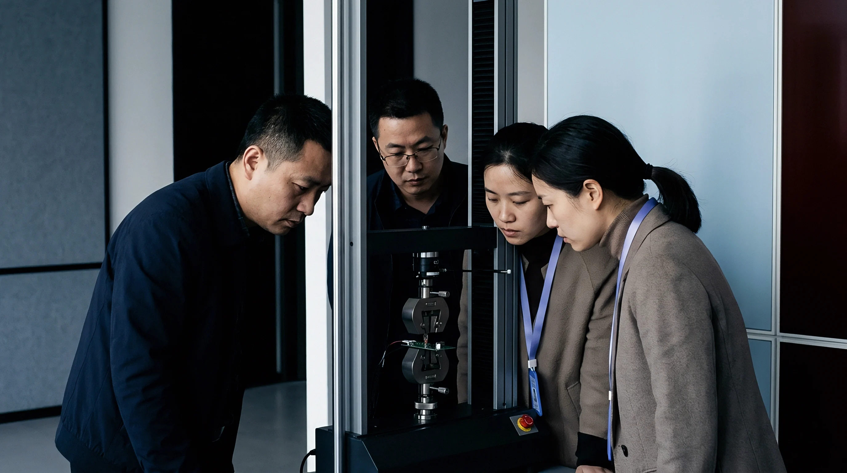
Detecting sub-micron void nucleation driven by spatial stress gradients requires advanced non-destructive and destructive analytical techniques. Standard X-ray inspection tools lack the spatial resolution needed to visualize sub-micron cavities prior to macroscopic coalescence. High-resolution laboratory X-ray nanotomography achieves spatial resolutions below 50 nanometers, enabling three-dimensional visualization of microvoid clusters buried deep within complex multi-layer microelectronic packages.
Cross-sectional analytical protocols rely heavily on Focused Ion Beam milling coupled with scanning electron microscopy. To prevent mechanical damage from altering fragile microvoid geometries during sample preparation, ion beam polishing must utilize low-beam-current final passes. Electron backscatter diffraction mapping performed concurrently with high-resolution electron microscopic imaging allows engineers to correlate physical microvoid locations directly with local crystal orientation gradients and grain boundary misorientation angles.
| Metrology Technique | Spatial Resolution Limit | Maximum Sample Depth | Sample Preparation Method | Primary Data Output |
|---|---|---|---|---|
| X-Ray Nanotomography | 40 nm | 1.5 mm | Laser Micro-Machined Pillar | 3D Void Distribution Matrix |
| Focused Ion Beam (FIB-SEM) | 5 nm | 50 µm | In-Situ Gallium Ion Cross-Section | 2D Microstructural Void Map |
| Scanning Acoustic Microscopy | 0.5 µm | 5.0 mm | Planar Immersion Polish | Interface Delamination Echo Map |
| EBSD Strain Mapping | 20 nm | Surface Only | Vibratory Cross-Section Polish | Micro-Strain Tensor Divergence |
Synchrotron X-ray diffraction provides non-destructive, real-time mapping of internal lattice strain fields under dynamic operating loads. By focusing high-energy X-ray beams down to sub-micron spot sizes, synchrotron measurements quantify local stress tensor components directly around geometric notches and material interfaces. These measurements yield empirical values for the spatial derivative of hydrostatic stress, validating numerical transport models against actual material behavior.
- Cut target packaging samples into micro-pillars using high-precision picosecond laser machining to preserve internal strain fields.
- Mount samples in dedicated thermal-mechanical testing stages capable of applying dynamic loads during X-ray exposure.
- Collect full 360-degree tomographic projection series at energy levels optimized for metallic phase contrast.
- Reconstruct three-dimensional volumetric datasets using filtered back-projection algorithms calibrated for phase-retrieval enhancement.
- Segment microvoid volumes using automated thresholding algorithms to extract quantitative void nucleation density metrics.
Standard quality specifications, such as IPC-7095D for BGA voiding, establish acceptance criteria based solely on two-dimensional planar void area percentages. These standards fail to regulate microstructural void nucleation induced by spatial stress divergence because sub-micron interface cavities accumulate without altering total planar void area until catastrophic separation occurs. Supplier quality agreements must explicitly mandate three-dimensional microstructural sampling protocols for high-reliability components.
Per IPC-A-610 Class 3 acceptance criteria, sub-surface interface microvoiding exceeding two percent of total contact length requires immediate lot containment and root-cause failure analysis.
Outlay

Commercial Consequences and Rework Economics
Microstructural void nucleation under high spatial gradient hydrostatic stress divergence introduces significant commercial risk to microelectronics and structural assembly manufacturing. Sub-micron cavities formed during burn-in screening or early operational cycles grow quietly during field use, resulting in latent product failures. These failures bypass standard factory quality gates because conventional end-of-line electrical testing and two-dimensional X-ray inspection cannot detect sub-surface vacancy clusters before complete structural fracture occurs.
Managing this risk requires adjusting operational spending, balance sheet reserves, and supplier inspection rhythms. When microvoiding forces product recalls or warranty returns, the financial damage extends beyond unit replacement costs to encompass field service calls, air freight expedites, product teardowns, and lost customer line availability. A failure rate under one-tenth of one percent in high-reliability power modules can eliminate the entire net margin of a assembly batch if post-packaging failure occurs after system integration.
The cost structure for addressing microstructural voiding splits between prevention expenditures and operational failure penalties. Investing in advanced substrate materials with closely matched thermal expansion coefficients increases front-end BOM costs by 12 to 18 percent. Upgrading plating line parameters to eliminate internal micro-void notches adds approximately 4 percent to substrate fabrication expenses.
These front-end costs remain far below the expenses associated with scrap, rework, and field failures.
Assume a high-reliability automotive assembly plant runs a quarterly volume of 250,000 power semiconductor modules at a unit fabrication cost of $45. Standard end-of-line testing identifies a 0.8 percent failure rate driven by unmitigated hydrostatic stress divergence at the substrate interface, forcing scrap and rework actions on 2,000 units. If these defective units pass factory testing and fail during vehicle operation, the cost shifts from simple $45 manufacturing scrap to a field warranty replacement cost of $1,200 per vehicle.
A failure escape rate of just 0.1 percent generates a direct warranty exposure of $300,000 per quarter, exceeding the annual cost of implementing advanced stress-divergence metrology and microstructural inspection routines across the entire supply chain.
Supplier contracts often fail to allocate financial liability for microvoiding defects correctly. Standard commercial terms class interface delamination under general workmanship clauses, allowing component vendors to dispute warranty chargebacks by asserting that assembly reflow profiles caused the microstructural degradation. Engineering purchase orders must specify exact microstructural void density thresholds, grain boundary micro-alloying concentrations, and mandatory thermal shock sampling protocols.
Linking component payment milestones directly to three-dimensional microstructural inspection verification prevents suppliers from shipping latent defect inventory that degrades in the field under operational stress gradients.