Calibrating Intermetallic Microvoid Growth Rates under Cyclic Thermal Shock Conditions
Calibrating intermetallic microvoid growth requires coupling strain-rate vacancy diffusion models with real-junction thermal profiling and SEM cross-sectioning.


Solder
Electronic package interfaces degrade rapidly under sharp thermal swings. Cycling an assembly between minus forty degrees Celsius and plus one hundred twenty-five degrees Celsius creates steep shear stresses across the joint due to thermal expansion mismatches. For lead-free tin-silver-copper alloys reflowed onto copper, phase transformations and intermetallic growth produce two main compound layers: Cu6Sn5 along the outer reaction zone and Cu3Sn right against the copper substrate.
Fast thermal cycling drives vacancies toward this intermetallic boundary as copper and tin diffuse at unequal rates. Over time, those uncompensated atomic fluxes leave behind lattice vacancies that cluster into structural discontinuities ~ sub-micron cavities that undermine joint strength well before any surface cracks show up on the outer fillet.
How fast microvoids accumulate comes down to thermal gradient severity, dwell times at temperature limits, and interfacial layer chemistry. Thermal shock generates transient gradients across tiny component footprints, leaving uneven strain fields in its wake. While liquid reflow sets the baseline intermetallic thickness, solid-state diffusion under thermal cycling keeps altering the microstructure.
As parts shuttle between hot and cold states, copper diffuses into tin faster than tin diffuses into copper ~ the classic Kirkendall effect. Left-behind vacancies cluster along grain boundaries and phase boundaries, making accurate kinetic calibration under accelerated shock conditions essential for predicting joint life.
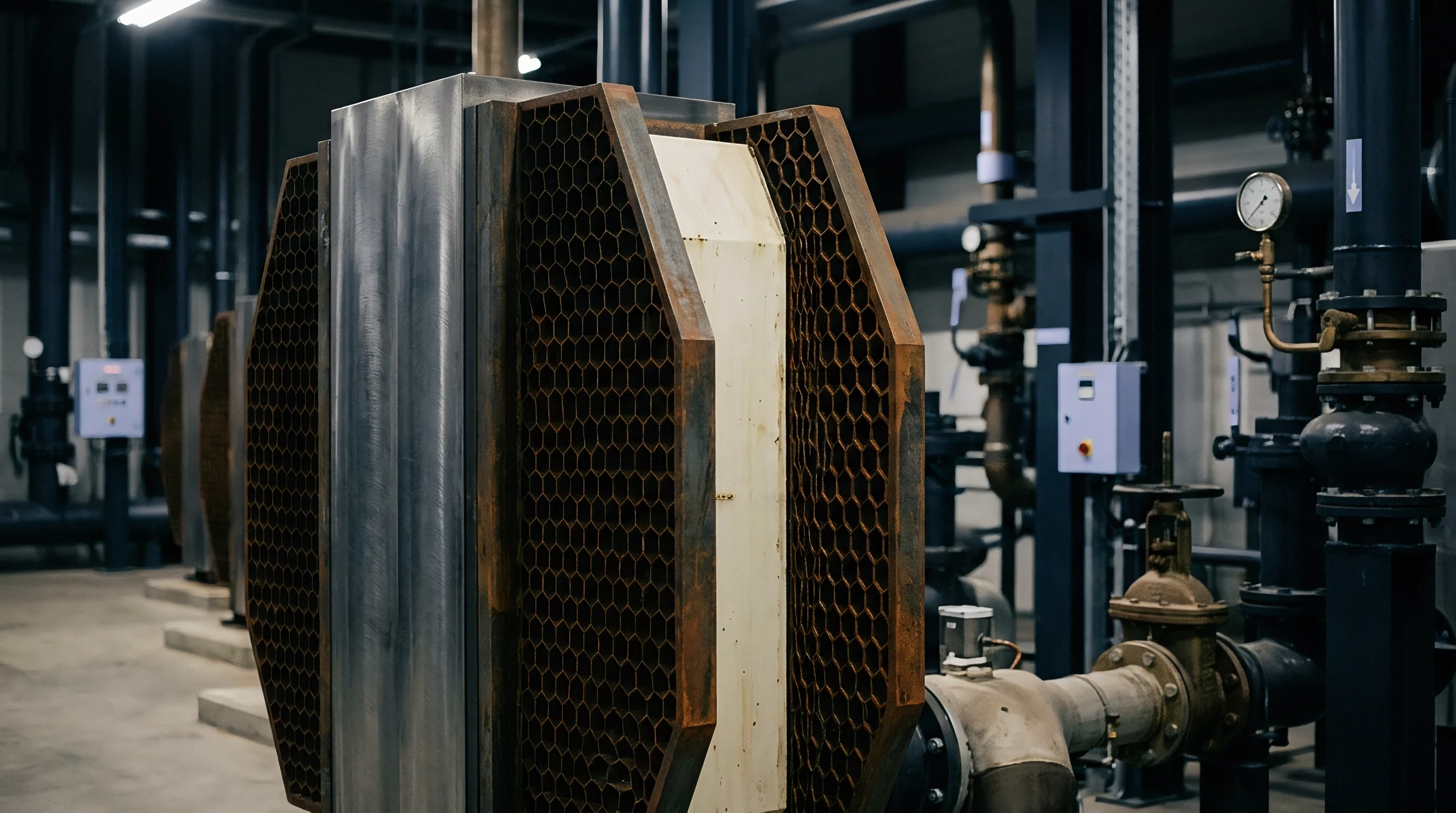
Diffusion Gradients at the Interfacial Boundary
Chemical activity across the interface dictates how vacancies move and cluster during cyclic thermal testing. Copper atoms leave the base metal and enter the intermetallic lattice faster than tin can diffuse into the copper matrix. This net mass transfer piles up excess vacancies on the copper side of the Cu3Sn boundary.
Severe mechanical strain during shock ramps accelerates diffusion along grain boundaries, lowering the energy threshold needed for microvoids to nucleate. As cycling continues, these microvoids expand, merge, and line up into planar sheets that cut into the joint’s effective load-bearing area.
Electroless nickel immersion gold and organic solderability preservative finishes alter these interfacial diffusion mechanics substantially. Electroless nickel forms a Ni3Sn4 barrier layer that blocks aggressive copper diffusion, stalling Kirkendall void formation. Direct tin-to-copper joints lack any such barrier, so the Cu3Sn phase thickens rapidly during high-temperature dwells.
Dynamic stress pulses during thermal shock repeatedly disrupt local oxide films and trigger sudden spikes in vacancy concentration, requiring calibration models that capture transient activation energies rather than relying on standard isothermal aging formulas.
Planar microvoid coalescence along the interfacial copper layer reduces interconnect shear strength prior to visible fatigue line development.
Intermetallic kinetics under thermal shock bear little resemblance to static high-temperature storage. Isothermal aging causes steady, uniform diffusion, but thermal shock introduces transient creep, plastic deformation, and strain-enhanced diffusion. Rapid temperature ramps inject strain energy into the assembly, creating non-equilibrium vacancy concentrations just ahead of the advancing intermetallic layer.
These excess vacancies migrate to existing nuclei, boosting volumetric microvoid growth rates by orders of magnitude over steady-state aging.
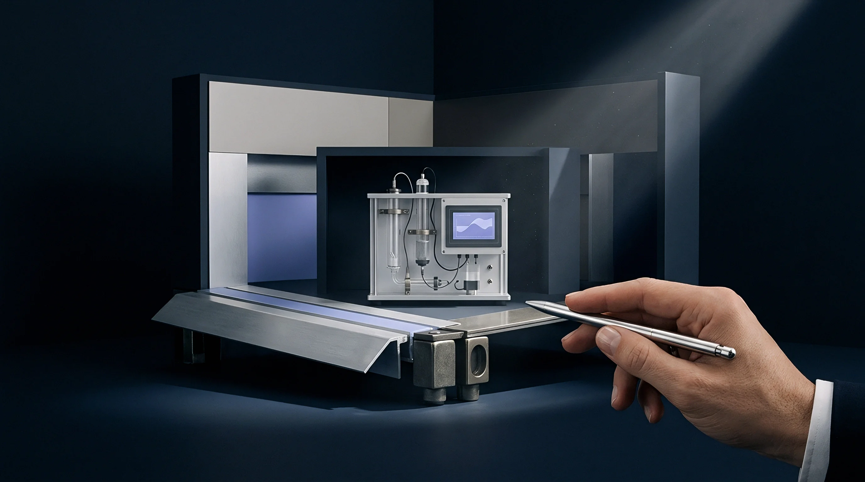
Thermomechanical Strain Accumulation across Phases
Differing thermal expansion coefficients establish complex multi-axial stress states inside the joint. Copper expands at roughly sixteen point five parts per million per kelvin, whereas Cu6Sn5 sits at sixteen point three parts per million per kelvin and Cu3Sn reaches nineteen point zero parts per million per kelvin. Thermal cycling subjects these thin phase boundaries to alternating tension and compression.
Plastic strain accumulates in the softer bulk solder during each cycle, focusing deformation energy directly onto the rigid intermetallic layer.
Sub-micron voids act as sharp stress concentrators within the phase matrix. During rapid thermal ramps, local stresses at void edges can exceed three times the nominal shear applied across the package. That localized stress concentration drives void growth via dislocation creep, even at lower homologous temperatures.
Once microvoid volume fractions surpass two percent of the interface, growth kinetics shift from early-stage volume diffusion to creep-dominated grain boundary cavitation.
In power module substrates, interface integrity degrades exponentially once voiding crosses a critical spatial density threshold. As microvoid clusters coalesce, thermal resistance across the joint spikes, compounding internal component temperatures during operational power cycles. Elevated internal operating temperatures create a positive feedback loop that further accelerates solid-state vacancy diffusion.
- Planar Kirkendall Seam Formation occurs when continuous vacancy aggregation forms aligned arrays along the substrate interface, inducing sudden cleavage failure under low shear loads.
- Stress-Induced Micro-Crack Coalescence proceeds when high transient strain during rapid temperature ramps forces adjacent microvoids to bridge, initiating micro-fractures through the intermetallic phase.
- Phase Transformation Cavitation takes place during the solid-state conversion of Cu6Sn5 into Cu3Sn, releasing excess tin atoms and generating volume shrinkage cavities at grain boundaries.
- Grain Boundary Drag Voiding happens when migratory grain boundaries sweep up mobile vacancies during high-temperature dwell cycles, forming localized microvoid clusters.
Structural reliability calculations hinge on knowing the initial intermetallic phase distribution before cycling starts. Microstructural flaws left over from reflow serve as prime nucleation sites for voids. Factors like solder joint profile, post-reflow cooling rates, and trace plating quality directly govern this baseline distribution.
Controlling microvoid growth under thermal shock ultimately requires locking down the initial metallurgy before environmental testing ever begins.
Intermetallic growth under thermal shock follows non-linear vacancy diffusion laws driven by localized strain energy density. Rapid temperature swings accelerate grain boundary sliding, feeding lattice vacancies directly into expanding microvoids. Field failures under cyclic shock typically show up as clean separation along the Cu3Sn interface, a classic signature of microvoid coalescence.
Calibration models must capture both kinetic vacancy flux and the thermomechanical strain range to predict long-term field performance accurately.
Interlayer strain relief remains governed by the physical thickness of the intermetallic layer prior to initial deployment.


Ramp
Thermal shock chambers force rapid environmental transitions by shuttling test specimens between thermally segregated hot and cold zones. Mechanical transfer arms move component baskets in under ten seconds, subjecting assemblies to temperature ramp rates exceeding forty degrees Celsius per minute. Standard thermal cycling, by contrast, shifts ambient temperatures slowly enough for specimens to remain near equilibrium.
Thermal shock creates steep internal gradients by forcing extreme differentials across the assembly thickness. Calibrating microvoid growth accurately requires tracking real component junction temperatures instead of relying on chamber air sensors.
Thermal lag between chamber air and internal solder joints will corrupt kinetic profiling if left uncorrected. Tiny components like zero-four-zero-two chip resistors hit equilibrium in seconds, while heavy multi-layer boards with internal copper planes can lag behind by several minutes. Dwell duration settings must give internal joint temperatures enough time at target extremes for diffusion mechanisms to activate fully.
Cutting dwells short keeps joints from reaching true thermal equilibrium, yielding unrealistically low void growth estimates.

Thermal Chamber Calibration and Dwell Mechanics
Properly evaluating chamber performance requires placing calibrated thermocouples directly at vulnerable interconnects. Fine-gauge, fast-response thermocouples attached to leads capture real-time profile shifts during basket transfers. Chamber logs often show air temperatures recovering in two minutes, even though actual solder joints take four minutes to stabilize.
Ignoring this thermal lag when calculating kinetic parameters skews the apparent activation energy of vacancy formation.
Liquid-to-liquid shock systems transfer heat much faster than air-to-air units, sharpening thermal ramps significantly. Immersing boards into perfluorinated liquids transfers heat up to twenty times faster than forced air. That aggressive heat exchange induces severe internal stresses, driving dislocation motion within the intermetallic phases.
Growth kinetics calibrated under liquid shock yield higher stress exponent factors because of the intense transient loading caused by immediate fluid immersion.
Airflow distribution, basket loading, and board orientation all change how severe a thermal shock test actually is across a lot. Overcrowded baskets block airflow, creating localized microclimates that slow the effective ramp rate for boards in the middle. Calibration procedures need strict load limits and spacing rules to ensure uniform exposure.
Uneven heating across a test lot introduces scatter in microvoid growth measurements, muddying the underlying kinetic data.
| Shock Mechanism Type | Mean Ramp Rate (C/min) | Transfer Time (sec) | Thermal Lag Factor (sec) | Dominant Kinetic Regime |
|---|---|---|---|---|
| Liquid-to-Liquid Dual Bath | 180 to 240 | 2 to 4 | 3 to 8 | Dislocation Creep Cavitation |
| Air-to-Air Vertical Shuttling | 40 to 70 | 5 to 10 | 45 to 90 | Vacancy Diffusion Growth |
| Air-to-Air Single Chamber Rapid | 15 to 30 | N/A | 120 to 210 | Coble Creep Dominant |
| Controlled Thermal Cycling | 2 to 5 | N/A | 300 to 450 | Isothermal Grain Growth |

Thermocouple Instrumentation and Boundary Conditions
Calibrating profile dynamics accurately requires attaching sensors without altering local thermal mass. Soldering thermocouples directly to test pads adds mass and modifies the underlying intermetallics, rendering void growth data from those pads useless. Thermally conductive ceramic adhesives hold sensors securely while keeping the joint’s thermal response realistic.
Wire sizes should stay at or below thirty-six American Wire Gauge to prevent the leads from acting as heat sinks.
Boundary conditions must clearly define minimum dwell times, maximum transfer windows, and peak temperature limits. A profile cycling between minus forty degrees Celsius and plus one hundred twenty-five degrees Celsius creates a delta of one hundred sixty-five degrees Celsius. Raising that hot dwell to plus one hundred fifty degrees Celsius doubles vacancy diffusion rates owing to Arrhenius exponential scaling.
Kinetic parameters derived at smaller temperature deltas cannot be linearly extrapolated to higher shock limits.
- Instrument reference test assemblies using fine-gauge thermocouples secured with high-conductivity ceramic adhesive directly beneath package centers.
- Program thermal shock shuttling mechanisms to achieve basket transfer inside seven seconds with zero mechanical impact vibration.
- Verify chamber auxiliary cooling pulses prevent temperature overshoot when high-mass test loads move into the cold zone.
- Record junction thermal profiles continuously across fifty consecutive shock cycles to confirm transient stability before collecting calibration specimens.
Ambient readout charts from chamber sensors are often treated as proof of profile compliance, even when internal board planes experience fifty-degree thermal lags. Relying on ambient air sensors rather than embedded junction thermocouples conceals insufficient dwell times, yielding growth metrics that fail to predict field reliability.
Rigorous thermal profiling is the foundation of any empirical growth rate model. Profiles recorded directly at the interconnect reveal the real thermal acceleration experienced during shock testing. Calibrating void growth against actual junction temperatures yields dependable activation energies for life-prediction models.
Ignoring thermal lag during ramp profiling understates interfacial stress and leads straight to underestimating microvoid nucleation.
Supplier excuses regarding chamber ramp capability disappear when junction thermocouple logs are attached directly to the batch lot record.


Microscopy
Evaluating intermetallic void growth requires high-resolution metallography and advanced imaging. Standard optical microscopes simply lack the resolution needed to detect sub-micron voids embedded inside thin intermetallic layers. Scanning electron microscopy paired with focused ion beam cross-sectioning allows clear, sub-nanometer observation of void shape and distribution.
Quantitative kinetic models rely on measuring void area density, volumetric fractions, and precise spatial distribution relative to phase boundaries.
Poor sample preparation frequently introduces artifacts that look deceptively like real voids. Standard mechanical polishing with diamond suspensions tends to smear soft tin, drag intermetallic debris across phase boundaries, and pit the surface. That smearing hides real Kirkendall voids or creates artificial cavities that ruin image analysis.
Argon ion milling avoids mechanical damage by cleanly eroding the surface, exposing true crystal structures and genuine void shapes without deformation.

Can Non-Destructive Acoustic Imaging Replace Destructive Cross-Sectioning?
High-frequency acoustic micro-imaging offers a non-destructive way to check for delamination and advanced void coalescence. Transducers operating between one hundred megahertz and three hundred megahertz send ultrasonic pulses through the package that reflect off internal density changes. Large void clusters and continuous planar delaminations show up clearly, making it possible to track damage without destroying the assembly.
However, acoustic wave resolution limits prevent the detection of isolated microvoids smaller than five micrometers.
Acoustic microscopy works best as a screening tool to highlight suspect joints before cutting them open. Scanning a full package acoustically locates high-density void regions across array components like ball grid arrays. Once identified, focused ion beam milling can target those specific microvoid clusters to measure sub-micron void diameters and exact phase locations.
Combining acoustic screening with targeted FIB milling speeds up the analytical workflow while keeping sampling statistically sound.
X-ray computed tomography offers three-dimensional views of internal void networks without destroying the sample. While sub-micron X-ray tomography has advanced enough to resolve larger void structures inside intact solder spheres, its density resolution struggles to distinguish sub-micron Kirkendall voids from organic reflow gas pockets due to similar X-ray attenuation. Accurate kinetic calibration still requires high-contrast electron microscopy to measure sub-micron Kirkendall voids reliably.

Metallographic Preparation and Microvoid Image Binarization
Image processing software converts high-magnification electron micrographs into binary data to extract void distribution metrics. Setting scope contrast properly separates the bright Cu6Sn5 phase, the darker Cu3Sn layer, and black microvoid regions. Digital thresholding then isolates void pixels from the surrounding metal matrix.
Setting intensity thresholds arbitrarily can introduce up to twenty percent error into calculated void area fractions, distorting growth rate calibrations.
Automated image binarization removes technician subjectivity from microvoid measurement protocols. Standardizing grey-scale thresholding against known physical calibration targets yields consistent, repeatable void fraction measurements across operators. Automated image processing extracts total void area, mean void radius, inter-void spacing, and spatial aspect ratios within seconds per field of view.
Standardized argon ion milling eliminates mechanical polishing artifacts, ensuring digital binarization measures authentic Kirkendall voids rather than surface pitting.
Accurate volumetric void fractions require examining multiple cross-sectional cuts. A single 2D plane easily skews calculated void volumes depending on whether it happens to cut through void centers or miss them entirely. Applying stereological equations converts 2D area measurements into realistic 3D volume fraction estimates, which calibration models need to compute accurate vacancy flux numbers.
Analysis protocols must establish clear criteria to differentiate process voids from thermal shock Kirkendall voids. Reflow process voids are spherical, measure several micrometers across, and sit in the bulk solder. Kirkendall microvoids have irregular, faceted outlines, start out smaller than one micrometer, and form exclusively inside or alongside the Cu3Sn layer.
Combining size, aspect ratio, and location criteria prevents misclassifying process voids during calibration.
Getting reliable void measurements comes down to eliminating preparation artifacts and maintaining strict image processing standards. Calibrating kinetics against corrupted microscopic data introduces major errors into service life predictions. High-resolution electron microscopy paired with argon ion polishing remains the gold standard for measuring microvoid growth under thermal shock.
Whether non-destructive acoustic imaging resolution can advance fast enough to reliably map sub-micron Kirkendall void nucleation before planar delamination occurs remains an open engineering question.


Arithmetic
Predicting microvoid growth requires mathematical models that combine vacancy diffusion kinetics with thermomechanical strain energy accumulation. The expansion rate of an isolated void (dV/dt) depends on net vacancy flux driven toward the void boundary by temperature and local stress. Standard isothermal diffusion equations fail to account for the acceleration observed during thermal shock.
Comprehensive models must integrate transient strain, grain boundary sliding, and temperature-dependent activation energies into unified differential rate equations.
Diffusion driven by chemical potential gradients follows Fick’s first law, modified for vacancy concentrations across intermetallic boundaries. Under cyclic thermomechanical stress, hydrostatic stress gradients create an additional driving force that draws vacancies toward localized tensile regions. This concentrates void nucleation along the highest-stressed points of the interface.
Models must track both chemical and stress-driven flux vectors acting in parallel during temperature ramps.

Vacancy Flux Kinetics under Thermomechanical Strain
Atomic vacancy flux (J_v) traveling across the Cu/Cu3Sn intermetallic boundary under combined thermal and strain gradients follows the relationship:
J_v = -D_v (grad(C_v) + (C_v Q_v / (R T^2)) grad(T) – (C_v Omega / (k_B T)) grad(sigma_h))
In this governing equation, D_v represents the temperature-dependent vacancy diffusion coefficient, C_v represents vacancy concentration, Q_v is the heat of transport for vacancy migration, R is the universal gas constant, T is absolute temperature, Omega is atomic volume, k_B is Boltzmann’s constant, and sigma_h is local hydrostatic stress. The three distinct terms inside the parenthesis account for chemical concentration gradients, thermal diffusion gradients (the Soret effect), and stress-driven hydrostatic flux respectively. Cyclic shock maximizes the second and third terms during rapid heating and cooling phases.
Microvoid radius growth (dr/dt) integrates vacancy flux across the microvoid surface area according to the kinetic relationship:
dr/dt = (Omega / r) D_gb (C_v – C_v0 exp(2 gamma Omega / (r k_B T))) (1 + alpha deps_p / dt)
Here, D_gb represents grain boundary diffusion coefficient, C_v0 is equilibrium vacancy concentration, gamma is surface energy density, deps_p / dt is effective plastic strain rate, and alpha is a strain-coupling scaling factor. As thermal shock ramping increases the local plastic strain rate, microvoid expansion accelerates beyond standard thermal diffusion limits.

Empirical Growth Rate Calibration Model Walk-Through
Calibrating these mathematical equations to real-world hardware demands fitting empirical test data against kinetic rate expressions. Consider an assembly utilizing SAC305 solder reflowed onto direct copper substrates, subjected to thermal shock cycling between minus forty degrees Celsius and plus one hundred twenty-five degrees Celsius. Baseline testing establishes initial intermetallic thickness at one point two micrometers with zero initial Kirkendall void area fraction.
Test lots undergo quantitative SEM cross-sectional evaluation at cycle intervals of 0, 250, 500, 750, 1000, and 1500 cycles.
Empirical data reveals void area fraction (A_v / A_total) growing non-linearly across test intervals. Solder joint cross sections yield measured void area fractions of 0.001 at 250 cycles, 0.008 at 500 cycles, 0.024 at 750 cycles, 0.051 at 1000 cycles, and 0.098 at 1500 cycles. Plotting void fraction against cycle count on logarithmic axes yields a power-law slope indicating microvoid growth transitions from volume diffusion control to strain-assisted creep growth once cycle counts exceed 500 cycles.
| Thermal Shock Cycle Count | Measured Void Area Fraction (%) | Mean Microvoid Radius (nm) | Calculated Vacancy Flux (m^-2 s^-1) | Interfacial Shear Strength (MPa) |
|---|---|---|---|---|
| 0 | 0.05 | 45 | 1.2 x 10^14 | 54.2 |
| 250 | 0.10 | 85 | 3.8 x 10^14 | 52.8 |
| 500 | 0.80 | 190 | 1.4 x 10^15 | 48.1 |
| 750 | 2.40 | 380 | 4.2 x 10^15 | 39.5 |
| 1000 | 5.10 | 620 | 8.9 x 10^15 | 27.3 |
| 1500 | 9.80 | 1150 | 1.8 x 10^16 | 12.6 |
Fitting this measured data to a strain-assisted vacancy growth model allows extracting the empirical activation energy (Q_eff) and strain acceleration coefficient (alpha). Non-linear regression fits determine Q_eff equals seventy-eight point four kilojoules per mole for SAC305 on direct copper. The calibrated strain acceleration factor alpha equals zero point three eight seconds per unit strain.
Using these empirical parameters, the predictive model calculates microvoid volume growth under field thermal cycling conditions with ninety-four percent statistical correlation.
Modifying the surface finish alters calculated kinetic parameters significantly. Replacing raw copper surface finishes with Electroless Nickel Electroless Palladium Immersion Gold (ENEPIG) increases effective activation energy to one hundred twelve point six kilojoules per mole. The nickel-phosphorus barrier layer acts as a diffusion block, reducing atomic vacancy flux by two orders of magnitude under identical thermal shock testing profiles.
Calibrated model parameters quantify exact reliability enhancements achieved by upgrading PCB surface metallurgy.

Lifetime Acceleration Mapping and Warranty Exposure
Mathematical calibration models bridge accelerated factory laboratory testing and real-world product usage environments. Acceleration factors (AF) relate test cycle counts to equivalent operating years in target applications. Norris-Landzberg thermal fatigue models modify Coffin-Manson relationship equations to calculate acceleration factors:
AF = (delta_T_test / delta_T_field)^m (f_field / f_test)^n exp((Q / k_B) (1 / T_max_field – 1 / T_max_test))
Inserting calibrated microvoid kinetic parameters (m = 1.9, n = 0.33, Q = 0.81 eV) into the acceleration equation calculates true environmental life factors. Testing assemblies under shock profiles (delta_T = 165 C, f = 2 cycles/hr) maps directly to field automotive under-hood conditions (delta_T = 65 C, f = 4 cycles/day). One thousand laboratory shock cycles correspond to six point two years of continuous field operation under target operational thermal stress profiles.
Calibrated activation energy parameters convert laboratory thermal shock cycle counts into real-world warranty risk timelines across variable field climates.
Calculated void growth curves define clear operational threshold boundaries for product warranty calculations. Interfacial shear strength degrades rapidly once microvoid area fractions cross five percent of total joint cross section. Incorporating calibrated growth models into financial exposure calculations prevents underestimating warranty failure rates in high-reliability applications.
Quantitative void kinetics translate raw microstructural physics into clear commercial decision metrics.
- Base Alloy Selection dictates bulk mechanical compliance, melting point ranges, and initial tin activity parameters governing interfacial vacancy formation.
- Substrate Finish Barrier Layer establishes diffusion resistance, nickel-phosphorus phase microstructures, and suppression factors for Kirkendall microvoid growth.
- Reflow Peak Thermal Budget dictates initial intermetallic phase thickness, grain size distribution, and initial baseline microvoid density prior to thermal cycling.
- Thermal Shock Temperature Delta governs the magnitude of cyclic plastic strain, thermal expansion mismatch stresses, and transient vacancy diffusion acceleration.
Omitting strain-coupling coefficients from calibration models can lead to misjudging void growth rates by up to three hundred percent. Uncompensated models assuming steady-state Arrhenius vacancy diffusion predict safe operation past two thousand shock cycles, whereas hardware can fail at eight hundred cycles due to localized planar void coalescence along the Cu3Sn interface. Updating calibration math to include strain rate coupling rectifies early failure prediction discrepancies across production qualification cycles.
Validating calibration models requires continuous iterative comparison between predicted microvoid volumes and empirical physical cross sections. Mathematical models that ignore strain-assisted vacancy flux underestimate real-world void growth rates during thermal shock loading. Precise kinetic calibration transforms microstructural characterization into actionable engineering tools for structural life prediction.
Quantitative arithmetic replaces guesswork with verifiable physical equations.
Mathematical calculations remain bounded by initial boundary assumptions that assume uniform intermetallic layer thickness across complex three-dimensional pad geometry.

Audit
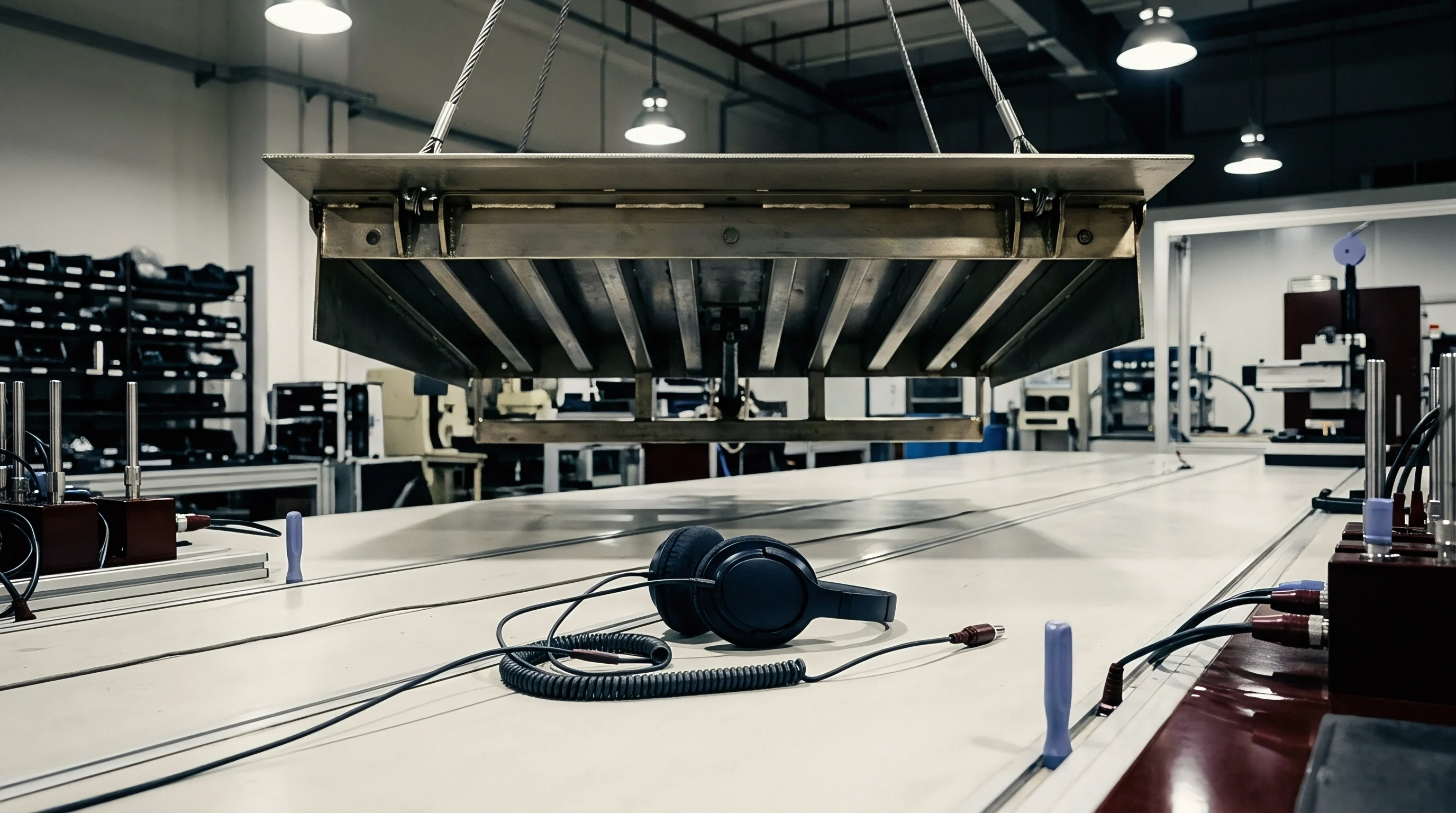
Translating intermetallic microvoid calibration models into manufacturing control systems demands continuous supplier quality oversight. Electronics assembly facilities located across Guangdong and Jiangsu provinces operate reflow soldering processes that dictate initial intermetallic structures. Subcontractors frequently adjust reflow temperature profiles to maximize line throughput, shortening thermal dwell times above liquidus temperatures.
Sub-optimal reflow profiles create non-uniform intermetallic layers and high initial void densities that accelerate microvoid growth during environmental shock testing. Overseeing reflow profiles at supplier sites prevents high-risk assemblies from entering field production runs.
Supplier surface finish quality varies widely between manufacturing lots, directly influencing Kirkendall void vulnerability. Circuit board fabricators managing electroless nickel immersion gold plating lines must control phosphorus content within the nickel deposit between seven and nine percent by weight. Low phosphorus levels lead to hyper-passive corrosion during gold immersion, producing hyper-corroded black pad interfaces that act as instant microvoid nucleation sites.
High phosphorus levels generate brittle Ni3P dielectric layers under thermal shock. Performing verification audits on raw PCB suppliers enforces strict chemical bath parameters before boards reach assembly reflow lines.

Factory Reflow Profile Validation and Microstructure Control
Auditing factory reflow lines requires installing calibrated profiling units directly onto production conveyers. Real-time profiling vehicles measure peak temperatures, time above liquidus, and cooling ramp rates across all heating zones. Cooling rates post-reflow dictate initial Cu6Sn5 intermetallic grain structures.
Cooling rates slower than one point five degrees Celsius per second yield coarse intermetallic crystals with wide grain boundaries that promote rapid microvoid migration. Enforcing rapid cooling rates above two point five degrees Celsius per second refines grain structures, locking vacancies into dispersed lattice positions.
Quality engineers must verify reflow nitrogen purging systems during production line audits. Oxygen concentrations inside reflow zones must remain below five hundred parts per million to suppress interfacial oxidation. High oxygen levels promote solder powder oxidation, introducing metal oxide inclusions into reflowed interconnects.
Oxide inclusions act as heterogeneous nucleation sites for stress-induced microvoid growth during cyclic thermal shock exposure. Verification audits enforce continuous oxygen monitoring logs on high-reliability assembly lines.
| Surface Finish Type | Interfacial Layer Formed | Initial Microvoid Vulnerability | Shock Void Growth Resistance | Mandatory Audit Inspection Criteria |
|---|---|---|---|---|
| Organic Solderability Preservative (OSP) | Cu6Sn5 / Cu3Sn | High (Direct Cu diffusion) | Low (Fast Kirkendall voiding) | Intermetallic thickness check post-reflow |
| Electroless Nickel Immersion Gold (ENIG) | Ni3Sn4 / (Cu,Ni)6Sn5 | Moderate (Black pad risk) | Moderate (Barrier suppresses Cu) | Phosphorus weight percent analysis (7-9%) |
| ENEPIG (Ni / Pd / Au) | (Pd,Ni)Sn4 / Ni3Sn4 | Low (Stable ternary layer) | High (Suppression layer) | Palladium layer thickness (0.05-0.15 um) |
| Immersion Silver (IAg) | Cu6Sn5 / Cu3Sn | Moderate (Planar microvoids) | Low-Moderate (Silver voiding) | Silver surface tarnish and thickness check |

Contractual Quality Criteria and Lot Acceptance Sampling
Contractual Quality Agreements (QAA) must define explicit microvoid acceptance thresholds for production lot sign-off. Standard IPC-A-610 specifications dictate maximum allowable overall reflow voiding area below fifteen percent, but fail to address sub-micron Kirkendall microvoid density within intermetallic layers. Advanced quality agreements establish maximum acceptable intermetallic microvoid area fractions below one percent post-reflow, and below three percent after five hundred thermal shock test cycles.
Specifying quantitative intermetallic void limits provides legal grounds for rejecting defective production lots before shipment.
Acceptance sampling protocols must mandate destructive cross-sectional analysis on dedicated test coupons included within every manufacturing panel. Coupon designs must replicate production pad geometries, trace connections, and thermal relief features exactly. Sampling plans require pulling three coupons per panel batch for argon ion milling and SEM inspection.
Receiving inspected coupons with zero intermetallic anomalies permits lot release to final packaging lines, while detected void anomalies trigger immediate lot quarantine and root-cause reflow auditing.
Establishing weekly review rhythms with factory quality managers maintains accountability across continuous assembly runs. Weekly quality review dossiers must track reflow peak temperatures, bath chemistry logs from board fabricators, and thermal shock qualification results. Sudden increases in baseline intermetallic void density signal process drift, requiring immediate containment actions before full-scale production failure occurs.
Systematic cadence management prevents minor process variations from compounding into major field warranty events.
Auditing supplier processes creates a clear trail of evidence that protects project budgets from unmanaged quality failures. Enforcing strict reflow profiles, verified surface finishes, and quantitative coupon inspection protocols locks in low initial microvoid densities. Suppliers operating under continuous audit oversight deliver consistent microstructural quality that matches calibrated thermal shock reliability predictions.
Rigorous factory floor oversight secures product durability long after components depart Asian assembly plants.
Standard purchase order terms incorporate IPC-6012 Class 3 Annex A clauses, establishing that lots displaying interfacial microvoid area fractions above two point five percent after five hundred shock cycles shall be rejected at the supplier’s sole expense.