Managing Intermetallic Growth in Advanced Substrate Copper Electrodeposition
Managing intermetallic growth in electrodeposited copper substrates requires strict additive control, low-temperature post-plating bakes, and nickel barrier layers.


Interface
Electrodeposited copper on advanced substrate layers interacts directly with tin-based solder alloys during thermal packaging operations. Solid diffusion drives phase growth. Solid-state reaction between pure copper and tin generates intermetallic compound layers that grow continuously under thermal stress.
The primary phase forming at the immediate electrodeposit interface during initial reflow is eta-phase Cu6Sn5. Substrate exposure to operational temperatures between 60 degrees Celsius and 150 degrees Celsius drives secondary phase transformation, forming epsilon-phase Cu3Sn between the original copper matrix and the Cu6Sn5 layer.
Copper diffusion rates through the intermetallic compound layers exceed tin diffusion rates by an order of magnitude. Copper atoms migrate outward toward the tin-rich solder interface, leaving behind unoccupied lattice sites within the copper matrix adjacent to the Cu3Sn interface. These lattice vacancies accumulate, coalescing into microscopic voids.
Void formation degrades the mechanical integrity of microvia target pads, surface-mount lands, and flip-chip solder bumps. Interfacial fracture toughness drops as void density expands along the planar boundary.

Solid State Diffusion Mechanisms
Thermal processing drives atomic movement across copper electrodeposits and tin interfaces after liquid solder reflow completes. Atomic flux across the interface depends on temperature, grain boundary density, and initial crystal lattice perfection. Interface energy governs void nucleation.
High atomic flux of copper toward the solder joint creates a net vacancy counter-flux toward the bulk copper substrate. When vacancy supersaturation reaches critical limits, void nucleation begins along crystallographic defects and impurity segregation sites.
Substrate copper grain boundary networks accelerate atomic transport compared to lattice bulk diffusion. Fine-grained electrodeposits with high grain boundary density exhibit higher overall intermetallic compound growth rates than coarse-grained copper structures. Interface mobility remains elevated as long as thermal energy fuels solid-state diffusion across phase boundaries.
Structural transformation from eta phase to epsilon phase consumes copper matrix volume while generating localized lattice strain.

Binary Phase Equilibrium at Electrodeposit Boundaries
Intermetallic compound growth proceeds through distinct thermodynamic stages controlled by thermal energy. Eta-phase Cu6Sn5 forms rapidly during liquid solder exposure at temperatures above 217 degrees Celsius. Epsilon-phase Cu3Sn nucleation requires sustained thermal activation, growing slowly at lower temperatures at the expense of both the copper substrate and the existing Cu6Sn5 layer.
Epsilon-phase formation consumes copper at a stoichiometric ratio of three copper atoms per tin atom, creating higher local volume shrinkage than eta-phase growth.
Substrate thickness loss directly correlates with total intermetallic layer thickness. In fine-line high-density interconnect circuit patterns where copper trace thickness measures under 10 micrometers, uncontrolled intermetallic growth consumes structural copper, altering signal trace impedance and reducing conductor cross-sectional area. Heat accelerates atomic species migration.
Managing phase boundary equilibrium demands controlling both electrodeposit microstructure and post-reflow thermal budgets.
Whether ultra-fine copper grain boundaries can be stabilized against thermal phase growth without introducing organic bath contaminants remains an open engineering question.


Bath
Aqueous solutions supplying copper ions to substrate panels rely on balanced acid concentrations to control deposition rates. Acid copper electrodeposition bath chemistries contain copper sulfate, sulfuric acid, hydrochloric acid, and proprietary organic additives. Plating current density alters microstructure.
Bath contamination alters deposit texture. Suppressors, accelerators, and levelers act simultaneously on the cathodic surface to control copper ion reduction kinetics, grain size, and microvia fill capability.
Organic additives regulate crystal growth rates across substrate panel topologies. Suppressor molecules, typically high-molecular-weight polyglycols, adsorb onto high-current-density surface areas, inhibiting copper ion reduction. Accelerator molecules, containing sulfur-functionalized organic thiols or disulfides, decrease local polarization resistance inside microvias to promote bottom-up filling.
Levelers select for high-curvature microstructures, preventing excess plating at via corners. Maintaining precise active chemical ratios suppresses non-uniform electrodeposit grain structures.

Additive Adsorption and Grain Refinement
Organic constituents added to electrodeposition tanks suppress high-current-density growth while accelerating fill inside microvia structures. Active carbon filtration lowers organics. Suppressors adsorb onto the substrate surface in the presence of chloride ions, forming a continuous barrier film that limits copper deposition speed.
Chloride ion concentrations below 40 milligrams per liter cause breakdown of the suppressor film, producing rough, nodular copper deposits with elevated dislocation densities.
| Constituent | Concentration Target | Operating Range | Defect Mechanism Outside Window |
|---|---|---|---|
| Copper Sulfate (CuSO4·5H2O) | 67 g/L | 60 – 75 g/L | Low concentration reduces plating speed and causes nodular growth |
| Sulfuric Acid (H2SO4) | 180 g/L | 165 – 195 g/L | Low conductivity causes poor throwing power in high aspect ratio vias |
| Chloride Ion (Cl-) | 50 mg/L | 40 – 60 mg/L | Sub-40 mg/L causes step plating; above 60 mg/L causes excessive additive breakdown |
| Organic Suppressor (PEG) | 12 mL/L | 10 – 15 mL/L | Depletion causes burning at high current density edges |
| Organic Accelerator (SPS) | 2.5 mL/L | 2.0 – 3.0 mL/L | Excess causes high lattice impurity codeposition and Kirkendall voids |
Elevated chloride levels exceeding 60 milligrams per liter precipitate cuprous chloride particles on the cathode. Particle entrapment generates crystallographic defects, increasing lattice strain within the electrodeposited copper matrix. Higher lattice strain drives faster solid-state diffusion when the substrate undergoes assembly soldering.

Organic Codeposition and Defect Nucleation
Breakdown products from organic suppressors and levelers become trapped inside the expanding metallic lattice during high-speed plating cycles. Organic fragments containing sulfur, carbon, nitrogen, and oxygen accumulate at grain boundaries. Thermal exposure during downstream assembly decomposes codeposited organic molecules, generating sub-nanometer gas bubbles and chemical impurities.
Excessive accelerator concentration in acid copper baths promotes microstructural lattice defects that accelerate thermal diffusion rates.
Sulfur impurities co-deposited from disulfide accelerators segregate directly to the copper-tin phase boundary during intermetallic compound growth. Sulfur segregation lowers the critical energy required for Kirkendall void nucleation. Continuous carbon treatment of the electrodeposition bath removes organic breakdown products before impurity codeposition reaches levels that compromise intermetallic interface reliability.
Maintaining carbon filtration on acid copper plating tanks prevents organic codeposition before grain boundary defects appear in microsection samples.


Foil
Electroplated metal sheets on high-density circuit boards exhibit dynamic crystal lattice behavior immediately following bath removal. Freshly electrodeposited copper undergoes self-annealing at room temperature over hours or days. Recrystallization releases internal lattice strain.
Cold storage delays self annealing. The microstructural transition involves spontaneous grain growth, where fine columnar grains transform into larger equiaxed crystallites.
Self-annealing kinetics depend on current density, bath additives, deposit thickness, and storage temperature. Fine columnar grains contain high defect densities, providing abundant diffusion pathways for copper atoms during subsequent thermal assembly. Equiaxed grain structures achieved after full recrystallization possess lower internal energy, fewer grain boundary paths, and improved thermal stability.
Controlling self-annealing timing before assembly reflow ensures consistent intermetallic growth behavior.

Grain Recrystallization Kinetics
Self-annealing transforms fine columnar structures into larger equiaxed crystallites at ambient room temperature over several days. Plating bath additives alter the driving force for recrystallization by modifying initial grain size and defect density. Unstabilized columnar deposits exhibit rapid grain growth, leaving residual micro-strains along grain boundaries if assembly reflow occurs prior to recrystallization completion.
Pre-assembly baking treatments at temperatures between 130 degrees Celsius and 170 degrees Celsius accelerate recrystallization, converting the copper microstructure into an equiaxed state within 60 minutes. Thermal stabilization reduces the vacancy concentration within the electrodeposited matrix before solder deposition occurs.
- Grain Size Equivalence Index verifies the structural homogeneity across high-density interconnect panel boundaries prior to thermal exposure.
- Self Annealing Stabilization Period measures the temporal delay required for electrodeposited microstructures to reach equilibrium crystallite dimensions.
- Preferred Crystallographic Orientation defines the ratio of low-energy lattice planes aligned parallel to the substrate interface surface.
- Impurity Codeposition Threshold tracks the atomic fraction of non-metallic elements incorporated within the electrodeposited matrix.

Crystalline Orientation and Vacancy Diffusion
X-ray diffraction analysis reveals that plated copper deposit textures influence atomic migration rates during thermal stress. Copper electrodeposits with a strong (111) crystallographic orientation present higher atomic packing density along the interface plane compared to deposits dominated by (200) textures. High packing density along (111) planes suppresses outward copper diffusion into tin solder layers during thermal aging.
A post-plating bake at 150 degrees Celsius for 60 minutes reduces Kirkendall void area fraction by 72 percent under subsequent 125 degree thermal stress.
Electrodeposition conditions that favor (111) crystalline orientation generate intermetallic compound layers with uniform planar interfaces. Lower vacancy generation rates along (111) interfaces prevent early void coalescence. Substrate manufacturing specifications demanding controlled plating parameters secure electrodeposits resistant to interfacial thermal degradation.
Failure to control self-annealing kinetics causes unpredictable interfacial shear resistance across microvia target pads during assembly reflow cycles.


Layer
Barrier coatings interposed between copper substrates and tin alloys physically arrest atomic migration across the joint. Electroplated nickel, electroless nickel, and cobalt alloy barrier films prevent direct contact between copper electrodeposits and tin-based solders. Barrier layers stop copper migration.
Substituting direct copper-tin contact with a nickel-tin interface alters intermetallic compound thermodynamics, suppressing Cu6Sn5 and Cu3Sn phase growth.
- Kirkendall Void Coalescence occurs when vacancy fluxes aggregate along planar grain boundaries beneath intermetallic layers under thermal aging.
- Planar Interfacial Microcracking originates from mechanical shear stress concentrated across dense arrays of microscopic boundary voids.
- Phosphorus Enrichment Embrittlement develops during solid-state aging when nickel reaction forms a weak nickel-phosphide layer.
- Hyper-Etch Barrier Dissolution stems from localized galvanic attack during chemical immersion preparation sequences.
- Asymmetric Phase Growth Failure arises when non-uniform barrier layer thickness allows localized copper migration into solder matrices.
Nickel reacts with tin solders to form Ni3Sn4 intermetallic layers at a growth rate significantly slower than copper-tin intermetallic growth. Lower growth rates reduce substrate copper consumption and eliminate Cu3Sn formation entirely, provided the barrier film remains continuous and uncracked throughout assembly life.

Nickel Diffusion Barrier Dynamics
Electroplated nickel films act as kinetic obstacles that slow down the reaction rate between copper substrates and tin solders. Deposition of nickel barriers from sulfamate or Watt’s plating baths produces fine-grained microstructures capable of blocking copper diffusion at operating temperatures up to 150 degrees Celsius. Barrier layer thickness must remain continuous across microvia sidewalls, pad edges, and trace features.
Discontinuities or pinholes in the nickel barrier layer allow localized copper diffusion into the tin solder joint. Localized diffusion forms isolated Cu6Sn5 nodules that penetrate through the nickel layer, creating stress concentration sites that induce fatigue cracking under thermal cycling.

Amorphous Structure Dopant Thresholds
Incorporating phosphorus into nickel deposits alters the crystal structure from polycrystalline to an amorphous state. Electroless nickel-phosphorus deposits containing 7 to 11 weight percent phosphorus provide superior diffusion resistance compared to crystalline electroplated nickel films. Amorphous nickel-phosphorus lacks grain boundary pathways, forcing copper migration to occur purely through slow bulk lattice diffusion.
IPC 6012E Class 3 specifies a minimum continuous barrier layer thickness of 1.27 micrometers to prevent copper migration into tin phases.
During solder reflow, nickel reacts with tin to form Ni3Sn4, displacing phosphorus from the reacting interface. Displaced phosphorus accumulates directly beneath the Ni3Sn4 layer, forming a thin, brittle nickel-phosphide layer (Ni3P). Excessive phosphorus accumulation generates structural weakness along the interface.
Controlling phosphorus bath concentrations prevents interfacial embrittlement while retaining barrier effectiveness.
Suppliers frequently attribute void formation to post-reflow storage temperature spikes rather than bath impurity accumulation during barrier electrodeposition.

Stress
Mechanical forces within advanced substrate structures originate from differential thermal expansion between dissimilar metal phases. Thermal shocks generate interfacial stress. Shear strength declines over time.
Substrate laminates, copper conductors, barrier metals, intermetallic compounds, and solder alloys possess distinct coefficients of thermal expansion. Repeated thermal excursions during operational life induce alternating shear and tensile stresses directly across intermetallic boundaries.
Kirkendall voids formed within the copper matrix adjacent to Cu3Sn layers multiply the damaging effect of mechanical stress. Voids reduce the effective load-bearing area of solder contacts, creating local stress intensity factors that accelerate microcrack propagation. Under high-strain environmental testing, interfacial cracks link adjacent voids, resulting in brittle planar mechanical failure.

What Controls Prevent Thermal Void Formation?
Pre-bake thermal treatments applied before assembly reflow stabilize the plated copper lattice by eliminating excess vacancies. Bath chemistry controls limiting organic impurity incorporation reduce void nucleation sites. Post-plating thermal bakes executed at 150 degrees Celsius for 60 to 120 minutes purge dissolved hydrogen gas and drive copper lattice recrystallization, stabilizing the microstructure before solder interface formation occurs.
Continuous monitoring prevents batch losses. Continuous carbon purification of plating baths prevents sulfur and organic contamination, ensuring grain boundaries remain free of low-melting-point species. Implementing automated chemical replenishment systems prevents bath constituent swings that generate microstructural lattice strains.

Mechanical Shear Degradation and Fractography
Interfacial microcracks propagate along Kirkendall void planes when joints undergo thermal cycle testing. Solder ball shear testing performed after isothermal aging reveals a transition from ductile bulk solder fracture to brittle interfacial fracture. The transition correlates directly with intermetallic layer thickness and interfacial void area fraction.
- Cast coupon mounts in cold-curing epoxy resin under vacuum to eliminate microscopic edge voids.
- Polish cross-sections sequentially down to 0.05 micrometer colloidal silica suspension to reveal true interfaces.
- Apply acidic ammonium persulfate etchant for four seconds to highlight grain boundaries without dissolving IMC phases.
- Measure intermetallic layer thickness across ten equidistant points using scanning electron microscopy at 5000x magnification.
- Record phase composition ratios using energy-dispersive X-ray spectroscopy to confirm stoichiometric stability.
When intermetallic layer thickness exceeds 4 micrometers, or when Kirkendall void area fraction along the copper-Cu3Sn boundary exceeds 15 percent, shear strength drops below acceptable reliability thresholds. Fractographic examination of failed surfaces using scanning electron microscopy shows dimpled void micro-void coalesced regions corresponding precisely to the original Kirkendall void plane.
| Phase Name | Chemical Formula | Crystal Structure | Formation Temperature | Diffusion Coefficient at 125°C |
|---|---|---|---|---|
| Eta Phase | Cu6Sn5 | Monoclinic / Hexagonal | Liquid reflow (217°C – 260°C) | 1.2 × 10^-13 cm^2/s |
| Epsilon Phase | Cu3Sn | Orthorhombic | Solid-state aging (60°C – 150°C) | 3.8 × 10^-14 cm^2/s |
| Delta Phase (Ni-Sn) | Ni3Sn4 | Monoclinic | Solid-state barrier aging | 4.1 × 10^-16 cm^2/s |
| Diffusion coefficients measured via secondary ion mass spectrometry across electrodeposited substrate interfaces after 500 thermal cycles. | ||||
IPC-6012E Class 3 microsection acceptance criteria reject coupon samples exhibiting continuous interfacial microcracking across more than eight percent of the plated land contact area.
Calculation
Financial outcomes in substrate manufacturing depend directly on managing chemical process windows to limit batch scrap rates. Scrap rates drive operational expenditure. Cross sections reveal hidden defects.
Yield loss resulting from intermetallic void failures during downstream qualification testing destroys profitability on fine-line substrate production runs. Establishing operational cost controls demands comparing bath maintenance expenses against thermal failure costs.
Consider a substrate fabrication plant producing 10,000 panel structures monthly for high-density package applications. Assume each panel yields 120 packaging units, totaling 1,200,000 units monthly. At a manufactured unit value of 2.50 USD, total monthly production value equals 3,000,000 USD.
Uncontrolled organic impurity accumulation in the acid copper bath typically increases assembly-level thermal stress rejection rates from 0.2 percent to 3.5 percent during high-reliability qualification testing.
Microsection Audit Economics
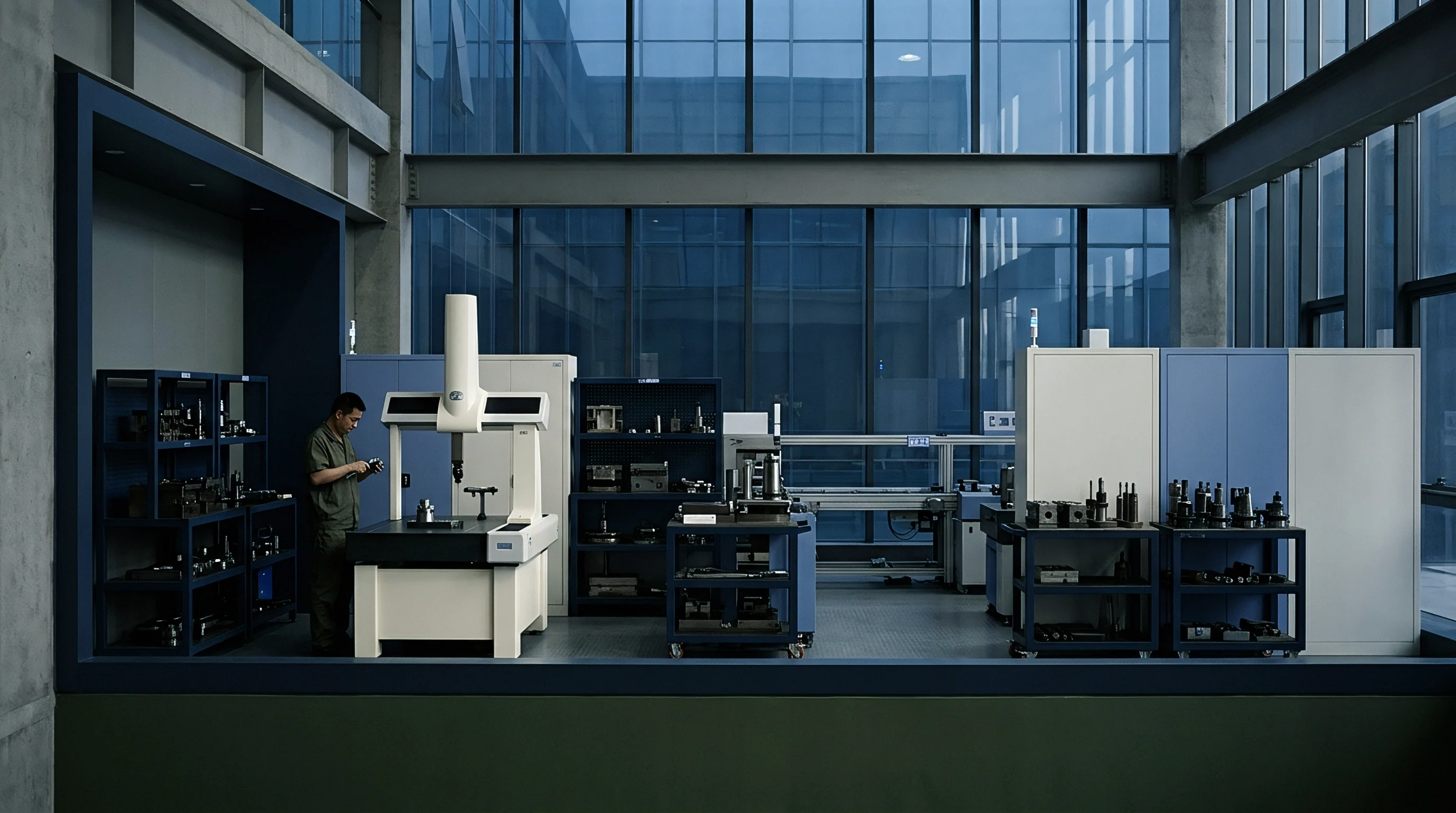
Quality assurance sampling requires continuous laboratory evaluation of metallographic cross-sections taken from production panel borders. Conducting regular microsection audits carries direct labor and equipment operational costs. A standard microsection inspection protocol involves extracting coupons from four corners per panel across five panels per plating lot, yielding 20 cross-sectional mounts for electron microscopy and energy-dispersive X-ray evaluation.
An inline carbon filtration unit for a 2,000-liter acid copper bath costs approximately 18,000 USD to install, with monthly consumable filter pack replacements costing 1,200 USD. Laboratory labor and equipment amortization for cross-sectional microsection testing amounts to 4,500 USD monthly per plating line. Total preventive operational expenditure equals 5,700 USD monthly per line.

Rework Thresholds and Process Cost Allocation
Determining whether to strip defective copper deposits or scrap whole production panels depends on thermal history limits. Allowing an uncontrolled acid copper bath to operate without carbon treatment leads to an elevated failure rate of 3.5 percent on a 3,000,000 USD monthly production run, resulting in a direct financial loss of 105,000 USD per month in scrapped substrate assemblies.
Comparing the monthly preventive quality control cost of 5,700 USD against the potential scrap loss of 105,000 USD demonstrates a net monthly savings of 99,300 USD per plating line. Investing in real-time chemical replenishment, active carbon treatment, and daily cross-sectional microsection audits protects operational yield against latent thermal degradation failures. The commercial balance depends on aligning active chemical controls with real-time microsection audits before copper grain defects convert into scrap.