Modeling Non-Isothermal Solid State Atomic Migration Rates across Non-Uniform Plated Substrate Boundaries
Non-isothermal atomic migration across plated substrate boundaries depends on controlling localized plating thickness steps and bath organic inclusions.

Gradient
Atomic transport across electroplated and electroless substrate boundaries is driven by coupled fields, with temperature variations creating localized diffusion hotspots. In high-density interconnects, ceramic direct bonded copper substrates, and advanced flip-chip packaging, solid-state migration driven by chemical potential differences combines directly with thermal transport forces. High current densities generate localized Joule heating, establishing steep temperature drops across microscale plating interfaces.
This thermomigration flux directly competes with or amplifies concentration-driven Fickian diffusion, altering vacancy distributions and microstructural stability.
Quantifying atomic movement across these interfaces requires solving multi-physics flux equations simultaneously. The total flux vector accounts for chemical concentration drivers, thermal forces, electric field stresses, and hydrostatic pressure variations across non-uniform plating layers. Localized gradients sharpen near substrate topography steps, thickness shifts from non-uniform plating density, and interfacial intermetallic compound layers.
Modeling these behaviors depends entirely on accurate, temperature-dependent transport coefficients.

Coupled Atomic Transport Field Equations
Mass transport in non-isothermal solid systems follows an extended Nernst-Planck flux relation. Net atomic flux J comprises four main components within the metallic substrate and plating layers:
J = -D nabla C – fracD C Q R T2 nabla T + fracD C Z e ρ jkB T + fracD C ΩkB T nabla σh
Where D is the temperature-dependent diffusion coefficient, C is atomic concentration, Q is the heat of transport governing thermomigration, R is the universal gas constant, T is absolute temperature, Z is the effective charge number for electromigration, e is elementary charge, ρ is electrical resistivity, j is the current density vector, kB is Boltzmann’s constant, Ω is atomic volume, and σh is hydrostatic stress. The diffusion coefficient’s temperature dependence follows an Arrhenius relationship:
D(T) = D0 expleft(-fracEakB Tright)
Here, D0 represents the pre-exponential frequency factor and Ea is the activation energy for atomic jumping. When thermal gradients across a plating interface exceed 103 K/cm, thermomigration matches isothermal concentration diffusion in magnitude. The direction of thermomigration depends on the sign of the heat of transport Q.
A positive heat of transport drives atoms toward cooler regions ~ leaving accumulated vacancies in hotter zones ~ while a negative value moves atoms toward the hotter boundary.

Thermal Gradient Concentration at Substrate Discontinuities
Uneven plating thickness across printed circuit board traces or ceramic substrate pads distorts local thermal profiles. Where electroplated copper or nickel layers narrow due to current shielding during deposition, electrical resistance climbs. These local resistance peaks create hotspots under heavy operating currents, generating localized, non-isothermal fields.
Thermal gradients concentrate around boundary steps, micro-voids, and grain boundary triple junctions. Local flux divergence (nabla · J) dictates where vacancies gather and material shifts. High negative flux divergence causes voids to nucleate, whereas positive flux divergence builds up mass, creating compressive stresses and potential whisker growth.
| Interface Couple | Pre-exponential Factor D0 (m²/s) | Activation Energy Ea (eV) | Heat of Transport Q (kJ/mol) | Effective Charge Z |
|---|---|---|---|---|
| Cu / Ni (Electroless) | 8.7 × 10⁻⁷ | 1.42 | +18.5 | -1.2 |
| Ni / Au (Immersion) | 2.1 × 10⁻⁶ | 1.15 | -12.3 | -0.8 |
| Cu / Sn (Electroplated) | 3.4 × 10⁻⁸ | 0.81 | +24.1 | -18.5 |
| Ni / Sn-3.0Ag-0.5Cu | 1.2 × 10⁻⁷ | 0.96 | +15.8 | -9.4 |
Interfacial thermal resistance across multilayer plated structures sharpens these temperature steps further. An immersion gold layer over electroless nickel, for instance, experiences distinct phonon mismatch scattering right at the nickel-gold boundary. Heat flowing perpendicular to this interface creates a discrete temperature drop across a sub-micron zone, producing an extreme thermal gradient that drives rapid atomic movement through the thin gold layer.
Interfacial Drift Kinetics under Non-Uniform Heat Dissipation
Non-isothermal boundary movement depends directly on spatial shifts in thermal dissipation. Substrate regions sitting directly over ceramic heat sinks shed heat rapidly, while suspended trace spans stay hot under continuous current load. Boundary drift velocity vdrift ties to net flux through atomic density N:
vdrift = fracJN
Discontinuities in substrate thermal conductivity break up linear temperature profiles across the boundary. When a copper trace runs from a solid ceramic backing onto a FR-4 dielectric pocket, heat flow shifts from axial conduction to perpendicular dissipation. The resulting thermal curvature (nabla2 T) produces a non-zero flux divergence even where atomic concentration is uniform.
The non-isothermal migration model must incorporate thermal gradient divergence terms to predict void formation locations accurately.
Simulating these field dynamics requires finite element formulations that update temperature, stress, and concentration fields at every discrete time step. Coupling these fields captures microstructural changes, as localized voiding shrinks the cross-sectional area ~ raising current density and heat dissipation in a self-reinforcing feedback loop. Solver stability relies on adaptive spatial mesh refinement near plating interfaces where gradient magnitudes peak.
An unresolved question is how dynamic thermal cycling above 100 Hz alters the effective heat of transport Q across non-equilibrium intermetallic boundaries during active phase transformation.


Grain
Microstructural features in plated metal layers dictate available atomic diffusion paths. Electroplated copper, electroless nickel-phosphorus, and immersion gold layers feature grain structures ranging from nano-crystalline columns to equiaxed recrystallized grains. High-angle grain boundaries act as fast-diffusion highways, with atomic jump frequencies several orders of magnitude higher than in the bulk crystal lattice.
Uneven plating conditions create spatial variations in grain size, crystallographic texture, and grain boundary density across the substrate surface. High current density zones during deposition yield smaller grains and higher grain boundary volume fractions. These microstructural variations open localized diffusion pathways, driving uneven atomic transport rates under thermal and electrical stress.

Grain Boundary Diffusion Short-Circuit Mechanics
Atomic movement along grain boundaries follows Harrison’s classification, divided into regimes A, B, and C based on how bulk diffusion length (Db t)1/2 compares to grain boundary width δ and grain diameter d. For micro-plated electronic substrate layers operating between 80°C and 150°C, regime B kinetics dominate.
Under regime B transport, diffusion moves simultaneously down grain boundaries and outward into adjacent bulk grains. The effective diffusion coefficient Deff follows Hart’s formulation for randomly oriented equiaxed grains:
Deff = Db + f Dgb
Where Db is lattice diffusivity, Dgb is grain boundary diffusivity, and f is the volume fraction of grain boundaries, approximated as f ≈ 3δ / d for an average grain diameter d and boundary width δ ≈ 0.5 nm. Columnar plating grains perpendicular to the substrate interface introduce diffusion anisotropy: transport along columnar boundaries parallel to the thermal gradient accelerates dramatically, while perpendicular migration remains governed by bulk lattice rates.

Intermetallic Nucleation at Plating Boundary Heterogeneities
Reactions between tin-based solders and substrate plating layers, like copper or nickel, form intermetallic compound (IMC) layers. Variations in plating thickness or surface roughness alter IMC nucleation density and growth morphology. While phase growth typically follows parabolic kinetics under isothermal conditions, thermal gradients skew growth rates between the upper and lower interface boundaries.
The formation of Cu6Sn5 and Cu3Sn phases creates distinct sub-layer boundaries with unique transport parameters. Solid-state diffusion through the Cu3Sn phase usually limits overall intermetallic growth. Under non-isothermal conditions, thermal gradient forces drive tin diffusion through Cu6Sn5 toward the copper interface, accelerating Cu3Sn layer growth on the hotter side while slowing it in cooler regions.
- Interfacial Kirkendall Voiding occurs when the outward flux of copper atoms into tin exceeds the inward flux of tin, leaving uncompensated vacancies that coalesce at the Cu3Sn interface.
- Columnar Grain Grooving creates localized channels that allow liquid solder or fast-diffusing species to penetrate deep into the plating layer, leading to premature barrier failure.
- Phase Pre-Emption alters compound growth sequences when steep thermal gradients suppress the nucleation of metastable intermetallic phases, favoring stable equilibrium phases instead.
- Organometallic Inclusion Entrapment along grain boundaries during plating lowers boundary cohesive energy and elevates grain boundary diffusion coefficients.

Phase Field Discretization of Irregular Barrier Layers
Modeling structural evolution across non-uniform plated interfaces requires diffuse-interface methods that avoid explicit interface tracking algorithms. Phase field models use continuous conserved variables for concentration c(mathbfr, t) alongside non-conserved order parameters ηi(mathbfr, t) to represent crystal orientations.
The total free energy functional F of the non-isothermal, non-uniform system combines bulk chemical free energy, gradient energy, and elastic strain energy:
F = intV left dV
Here, f0 is local chemical free energy density, κc and κη are gradient energy coefficients, and eelastic is elastic strain energy density from lattice mismatch and thermal expansion anisotropy. Over time, the concentration field evolves according to a Cahn-Hilliard equation modified for thermomigration:
fracpartial cpartial t = nabla · left
Where M(c, T) is spatial atomic mobility tied to the local interdiffusion coefficient. Spatial discretization via high-order spectral methods or adaptive finite elements enables detailed modeling of Kirkendall voiding, grain boundary grooving, and intermetallic growth along irregular plating topographies.
Columnar plating structures with grain boundaries aligned parallel to operational heat flux represent the fastest path to latent barrier layer failure.
Grain boundary density is inversely proportional to local bath current density during deposition, establishing a direct physical link between electroplating parameters and long-term migration resistance.

Gauge
Model verification requires high-resolution metrology capable of isolating atomic transport across sub-micron boundary layers under active or post-stress thermal gradients. Standard optical cross-sectioning lacks the resolution to map nanometer-scale diffusion profiles or void distributions. Analytical workflows instead combine focused ion beam sectioning, transmission electron microscopy, electron probe microanalysis, and in-situ thermal stage testing.
Characterizing non-isothermal migration requires controlled thermal stress testing paired with quantitative chemical profiling. Establishing accurate baselines requires mapping plating thickness, surface roughness, and grain structures prior to environmental testing.

How Do Thermal Gradients Accelerate Interfacial Kirkendall Voiding?
Thermal gradients drive directional vacancy fluxes that add directly to the intrinsic Kirkendall vacancy flux created by unbalanced elemental diffusivities. When electroplated copper reacts with tin solder, copper diffuses outward faster than tin moves inward. This net mass transport causes a counter-flow of lattice vacancies back toward the copper interface.
Superimposing a temperature drop across this interface alters vacancy supersaturation. If heat flows from the tin side into the copper substrate, thermomigration pushes copper atoms away from the hot copper interface, accelerating outward migration. Vacancies accumulate rapidly at the Cu/Cu3Sn interface, driving void nucleation and growth far beyond isothermal rates.
Reversing the gradient suppresses vacancy supersaturation and slows void formation.
| Measurement Technique | Spatial Resolution | Detection Limit | Primary Measurement Capability | Operational Limitation |
|---|---|---|---|---|
| FIB-SEM Slice & View | 5 nm | 1.0 at.% | 3D void distribution and micro-crack mapping | Destructive; potential ion beam damage artifacts |
| TEM / STEM-EDS | 0.2 nm | 0.1 at.% | Atomic-scale chemical profiling across phase boundaries | Extremely small sampling volume; sample preparation artifacts |
| EPMA Line Profiling | 500 nm | 0.01 at.% | Precise quantitative elemental concentration tracking | Spatial resolution blur across sub-micron layers |
| In-Situ Synchrotron XRD | 100 nm | Phase specific | Real-time strain mapping and intermetallic phase growth | Requires high-energy beamtime access and specialized stages |

In-Situ Metrology Protocols for Interfacial Drift Measurement
Calibrating thermomigration parameters requires specialized test vehicles exposed to controlled thermal fields. Substrates with micro-fabricated heaters and integrated thin-film RTD sensors allow continuous monitoring of local thermal gradients during stress testing.
Measuring boundary displacement and vacancy concentration relies on standardized sample preparation and analytical steps. The profiling protocol proceeds sequentially to ensure repeatable parameter extraction.
- Fabricate test coupons with micro-plated substrate trace arrays containing non-uniform plating thickness steps ranging from 1.0 to 5.0 microns.
- Map baseline thickness across all trace step features using high-resolution X-ray fluorescence.
- Section control samples using a focused ion beam to map initial grain size and interfacial boundary profiles.
- Mount the test vehicle on a calibrated in-situ thermal stage capable of maintaining 104 K/cm gradients under ultra-high vacuum.
- Power the internal micro-heaters with direct electrical current, raising local hot-spot temperatures to 150°C while chilling the base to 30°C.
- Monitor loop resistance continuously to capture early vacancy condensation and micro-cracking events.
- Remove samples at set intervals (250, 500, and 1000 hours) for quantitative EPMA elemental mapping and FIB-SEM cross-sectional analysis.
- Extract effective heats of transport Q and vacancy diffusion parameters by fitting finite element models to measured concentration profiles.

Worked Example: Two-Barrier Diffusion Profiling under Thermal Bias
A comparative trial evaluated Electroless Nickel Immersion Gold (ENIG) against Electroless Nickel Electroless Palladium Immersion Gold (ENEPIG) finishes on ceramic direct bonded copper substrates under thermal stress.
Test parameters specified a thermal gradient of 2.5 × 10³ K/cm across the plated boundary layers, maintaining a baseline interface temperature of 135°C for 750 hours. The ENIG structure used a 4.0,μm electroless nickel-phosphorus layer (8.5 wt% P) capped with 0.05,μm immersion gold. The ENEPIG structure shared the same nickel plating but included a 0.10,μm electroless palladium buffer layer before gold immersion.
Post-test EPMA profiling revealed clear differences in nickel transport. In the ENIG structure, gold diffused rapidly along nickel grain boundaries toward the substrate interface while nickel migrated outward into the solder joint. This created a broad Ni3Sn4 intermetallic layer marked by hyper-passive nickel corrosion and Kirkendall voiding, with 3D FIB-SEM tomographic reconstruction showing a vacancy volume fraction of 6.2% across the interface area.
The ENEPIG structure proved far more stable. The palladium intermediate layer served as an effective barrier, suppressing nickel diffusion and keeping the vacancy volume fraction below 0.4% after 750 hours. Quantitative modeling confirmed that the palladium buffer raised the effective thermodynamic activation energy barrier for nickel migration from 1.15 eV to 1.68 eV, cutting net mass flux by over an order of magnitude under the same thermal gradient.
ENEPIG barriers reduced interfacial Kirkendall void accumulation by 93% compared to standard ENIG under a 2500 K/cm thermal gradient.
Uncalibrated FIB ion currents during failure analysis can create artificial amorphous surface layers, distorting TEM energy-dispersive X-ray spectroscopy line profiles on immersion gold boundaries.

Plating
Manufacturing electroplated and electroless substrate finishes requires tight control over bath chemistry, hydrodynamics, and electric field distribution. On the shop floor, small process variations introduce microstructural non-uniformities that degrade boundary migration resistance. Plating lines across manufacturing hubs in Guangdong and Zhejiang often exhibit subtle process shifts that turn into latent field reliability defects under thermal gradient loading.
Bath additives ~ brighteners, levelers, and suppressors ~ regulate deposition rates across surface topographies. Off-target concentration ratios or organic contaminant buildup create localized inclusions along grain boundaries. These organic inclusions alter local activation energy for solid-state diffusion, opening fast paths for atomic migration.
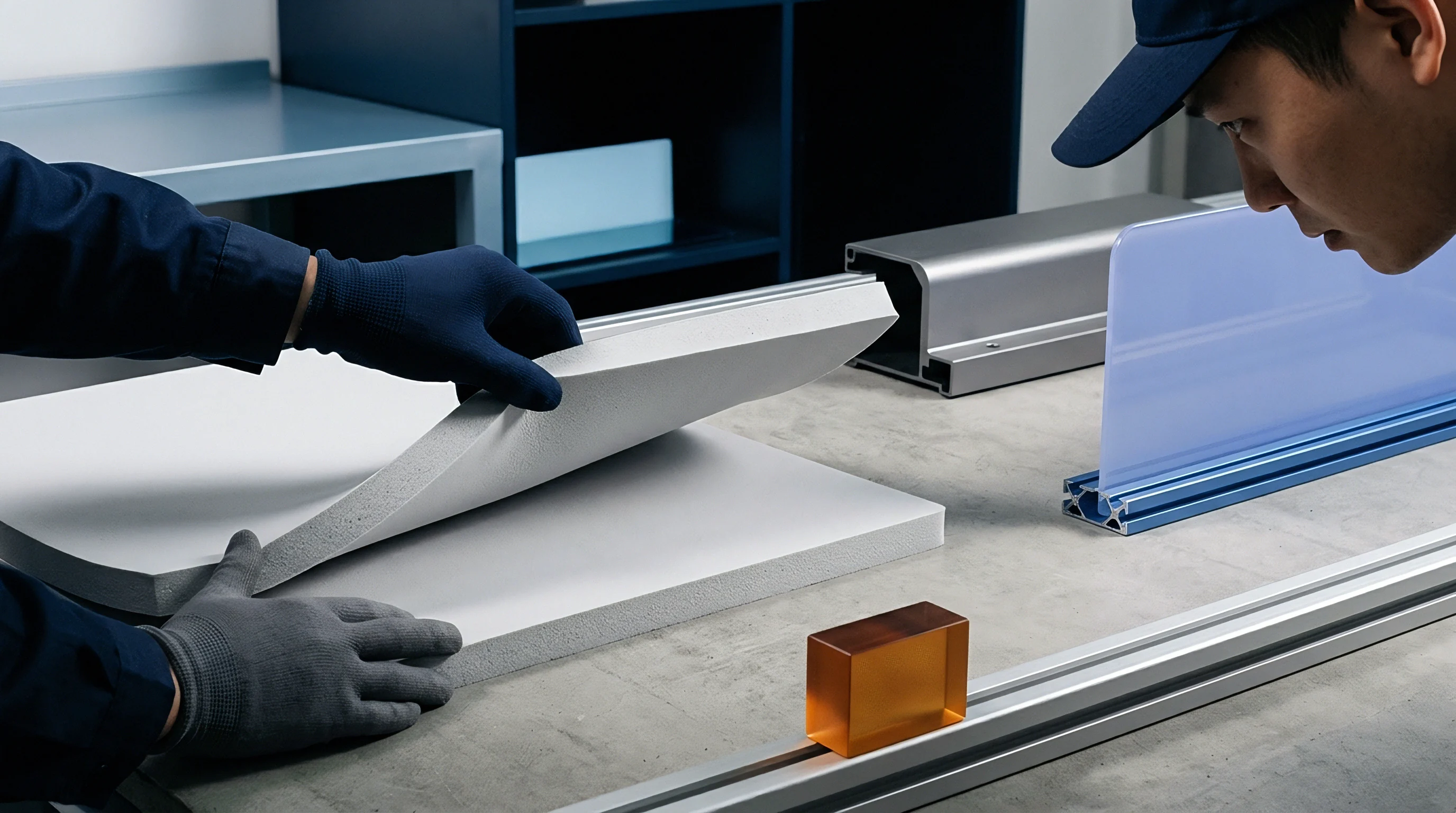
Bath Chemistry Control and Additive Inclusions
Electroplating baths rely on organic additives to keep deposits uniform. Leveling agents adsorb preferentially on high spots to suppress local growth, while brighteners speed up deposition in recessed features. When leveler concentrations drop below control limits, plating thickness varies widely across fine-pitch traces.
Organic additives break down over extended plating runs under continuous current exposure. These decomposition products accumulate in the bath and co-deposit with metal ions along grain boundaries. Incorporating carbon, sulfur, and hydrogen into electroless nickel or electroplated copper degrades lattice perfection.
Higher carbon concentrations at grain boundaries correlate with elevated grain boundary diffusivity Dgb, lowering activation energy Ea for intermetallic growth.
- Leveler Concentration Drift creates micro-scale thickness steps across high-density interconnect pads, concentrating stress and localizing thermal gradients.
- Chloride Ion Imbalance in acid copper baths shifts crystalline grain orientation away from diffusion-resistant (111) planes toward fast-diffusing (200) textures.
- Bath Organics Breakdown increases sulfur co-deposition along grain boundaries, accelerating nickel dissolution during high-temperature reflow.
- Phosphorus Content Fluctuation in electroless nickel deposition alters amorphous-to-crystalline transition temperatures, shifting stress states during operational heating.

Geometrical Current Density Non-Uniformity on Substrate Panels
Current density distribution depends on panel layout geometry, thief ring design, and anode positioning within the cell. Panel edges experience higher electric field density than central areas, creating local current density spikes unless properly shielded.
High current density deposition yields smaller grains and higher grain boundary density. Low current density zones near panel centers produce coarse grain structures and potential thickness deficiencies. A panel varying from 2.5,μm thickness at the center to 6.0,μm at the edge introduces inconsistent diffusion kinetics across identical circuits in the same lot.

Factory Operating Rhythm for Process Verification
Consistent plating quality requires a structured shop-floor rhythm that pairs automated process telemetry with mandatory physical verification. Relying solely on weekly supplier batch reports leaves operations blind to unannounced bath shifts and thickness drift.
An effective verification rhythm combines daily automated bath analysis, weekly cross-sectional metrology, and bi-weekly thermal stress validation. Plant quality controls rely on strict monitoring protocols to catch plating variations before substrates hit assembly packaging lines.
- Require real-time cyclic voltammetry stripping (CVS) analysis of organic additives every four hours to hold brightener and leveler concentrations within ± 5% of target.
- Run automated XRF thickness mapping on a 36-point grid across five sample panels per shift, enforcing a maximum variation threshold of Cv < 0.06.
- Section and polish two sample coupons per plating line daily to evaluate grain structures via cross-sectional optical and SEM analysis.
- Measure phosphorus weight percentage in electroless nickel baths using ICP-OES twice per shift, holding limits to 8.0–10.5 wt% P.
- Conduct weekly thermal shock testing (-55°C to +125°C, 100 cycles) on coupon cross-sections to verify interfacial adhesion and check for micro-voiding prior to lot release.
Standard supplier quality certifications rarely guarantee uniform atomic migration resistance across non-isothermal operating regimes.
A 20% leveler shift is sometimes treated as standard for high-volume commercial runs, but non-uniform plating thickness creates local hotspots that drive rapid Kirkendall voiding under power.


Exposure
Latent atomic migration failures across non-uniform substrate boundaries carry major commercial risk. Unlike manufacturing defects caught during end-of-line testing, thermomigration and stress-assisted diffusion issues take months or years of field operation to manifest. High thermal gradient environments ~ such as automotive power electronics, industrial motor drives, and hyperscale compute acceleration cards ~ accelerate these failure modes, driving field returns, sudden product shutdowns, and warranty liabilities.
Quantifying financial exposure means combining physical atomic flux models with statistical reliability distributions. Calculating expected failure rates over product lifespans allows engineering teams to price risk accurately, set aside appropriate warranty reserves, and defend technical specifications during contract negotiations.

Financial Modeling of Latent Interfacial Degradation
Field failure probability over time t follows a cumulative Weibull distribution F(t) modified by acceleration factors from the physical transport model:
F(t) = 1 – expleft
Where β is the Weibull shape parameter (typically β > 2.5 for wear-out degradation like Kirkendall voiding), η0 is characteristic life under baseline conditions, and AF is the multi-physics acceleration factor combining Arrhenius thermal acceleration with thermal gradient forces:
AF = expleft · expleft
Here γ is an empirical coupling coefficient for thermomigration gradient severity. Plugging finite element model predictions for local thermal gradients (nabla T) and peak interface temperatures (T) into the acceleration factor lets financial analysts project field return volumes across warranty windows.
| Operating Strategy Option | Plating Oversight Cost (per 10k Units) | Predicted 3-Year Field Failure Rate | Estimated Field Rework Liability | Net Financial Risk (per 10k Units) |
|---|---|---|---|---|
| Standard Commercial Plating (No Gradient Control) | $0 | 4.2% | $630,000 | $630,000 |
| Enhanced XRF & Bath Control (Standard Tolerances) | $12,500 | 1.1% | $165,000 | $177,500 |
| Advanced ENEPIG + Full Non-Isothermal Audit Rhythm | $38,000 | 0.03% | $4,500 | $42,500 |

Contractual Yield Guarantees and Rework Penalty Mechanics
Standard procurement agreements tied to basic IPC-610 or IPC-6012 criteria fail to protect buyers against latent migration defects. Traditional standards focus on surface appearance, baseline solderability, and average plating thickness, overlooking grain boundary orientation, organic contamination limits, and local thickness steps.
Adding explicit solid-state stability requirements to master supply agreements pushes risk back onto the plating vendor. Quality contracts need to look beyond simple thickness averages and enforce strict microstructural and bath chemistry stability metrics.
Contracts should explicitly state that any lot with thickness variations exceeding Cv = 0.05 across a single panel, or carbon co-deposition above 150 ppm along nickel-gold interfaces, will be rejected at the vendor’s expense ~ with the vendor covering all air freight and secondary assembly rework costs triggered by latent interface failures.