Mechanisms of Stress Gradient Coupling and Interfacial Delamination under Extreme Thermal Gradients
Interfacial delamination under extreme thermal gradients is driven by edge peel and shear stresses; mitigate via compliant interlayers and strict acoustic bounds.
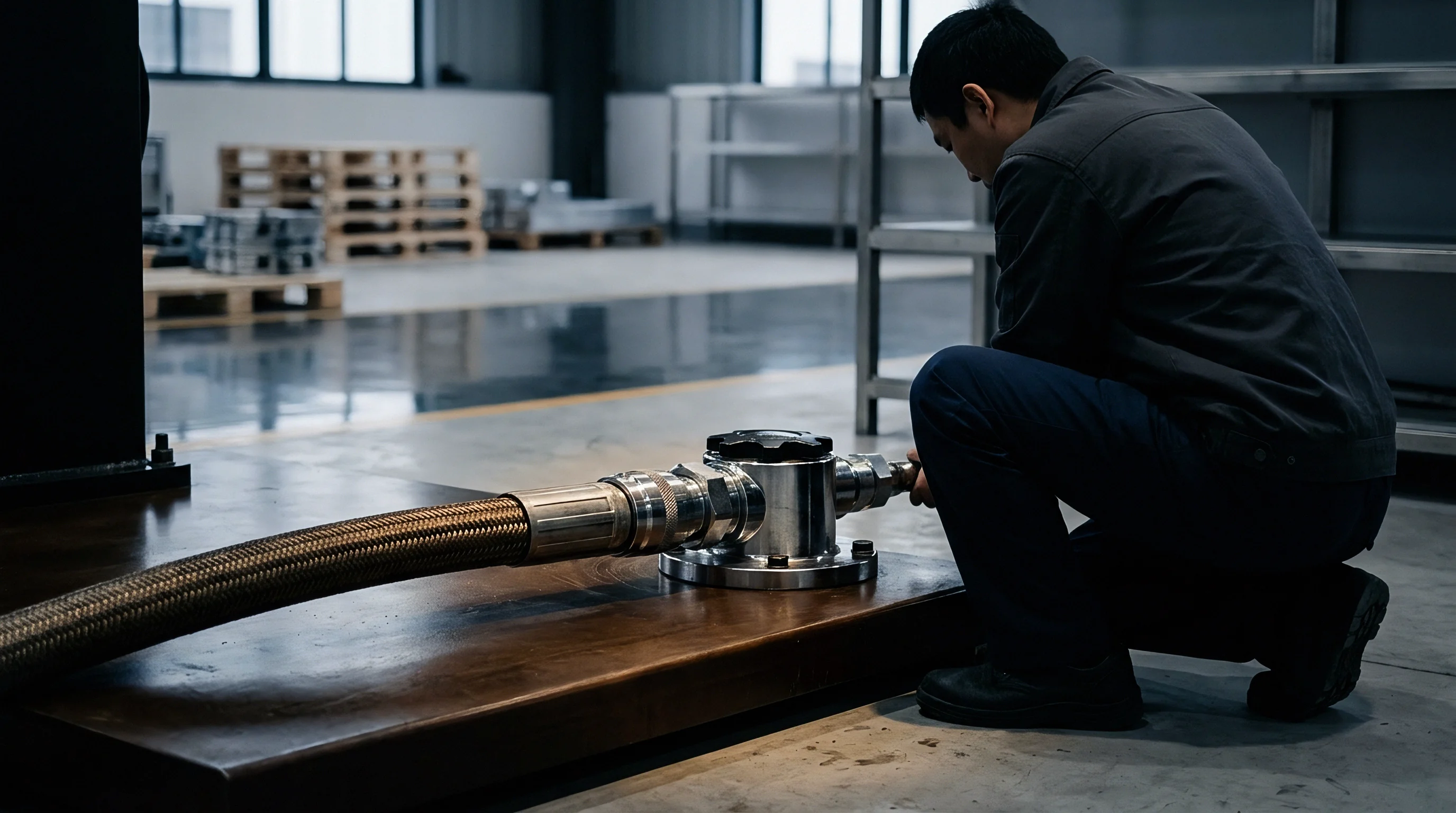

Flaw

Subsurface Shear Driven by Thermal Wavefronts
Thermal shocks exceeding 800 Kelvin per second across thin bonded assemblies induce steep mechanical gradients that concentrate at planar joints. In laminated power electronics and thermal barrier coatings produced in regional packaging hubs, these shocks trigger premature interfacial debonding before bulk materials exceed their nominal yield points. High localized heat flux drives differential volumetric expansion between adjacent material planes.
The resulting elastic displacement mismatch forces the joint to carry severe out-of-plane peel and in-plane shear strains simultaneously.
When high transient heat flux enters a multilayer assembly, heat diffusion remains confined to a thin boundary layer near the exposed surface. The unheated substrate stays rigid while the top layer attempts rapid lateral expansion. This physical constraint generates biaxial compressive stresses exceeding 400 megapascals in the expanding layer, balanced by steep tensile stress fields directly beneath the interface.
The localized gradient of this mechanical field drives mode-mixity shifts at embedded crack tips, promoting rapid, unstable crack advance along weakly bonded regions.
An unconstrained thermal expansion mismatch drives interface shear stress proportionally to the local temperature derivative along the through-thickness axis.
The severity of interfacial delamination depends directly on the mismatch between the thermal expansion coefficients of the joined materials. Ceramic-metal joins such as direct bonded copper or silicon nitride power substrates frequently encounter thermal expansion differentials greater than ten parts per million per Kelvin. Under steep through-thickness thermal gradients, this disparity produces strong peeling moments along free edges.
Microcracks then nucleate at pre-existing porosity sites and propagate under mixed-mode loading conditions.

Driving Force across Dissimilar Elastic Media
Fracture mechanics across bimaterial interfaces requires tracking the complex stress intensity factor along the crack path. The local mechanical driving force depends on both the elastic modulus mismatch and the differential thermal expansion coefficients. Dundurs parameters quantify this elastic disparity, determining how shear and normal stresses couple at the crack tip.
When extreme heat inputs alter the local temperature field, the thermal gradient acts as an internal body force that directly feeds the energy release rate.
Conventional structural assessments assume isothermal stress distributions, overlooking transient boundary layer effects. During rapid heating cycles, interfacial shear stress peaks sharply near edges and structural discontinuities. If the calculated energy release rate exceeds the critical interfacial fracture energy of the material pair, delamination begins without any externally applied mechanical load.
The crack follows the path of lowest fracture toughness, running along the boundary or kinking into the lower-modulus substrate.
A supplier who provides shear test data collected only under uniform furnace equilibrium measures zero gradient coupling. Production lines relying on such static data experience unpredicted field failures during dynamic thermal cycling. Interfacial debonding accelerates exponentially under steep temperature drops, where the surface contracts rapidly over a warm, expanding core, reversing the sign of the edge peel stress.
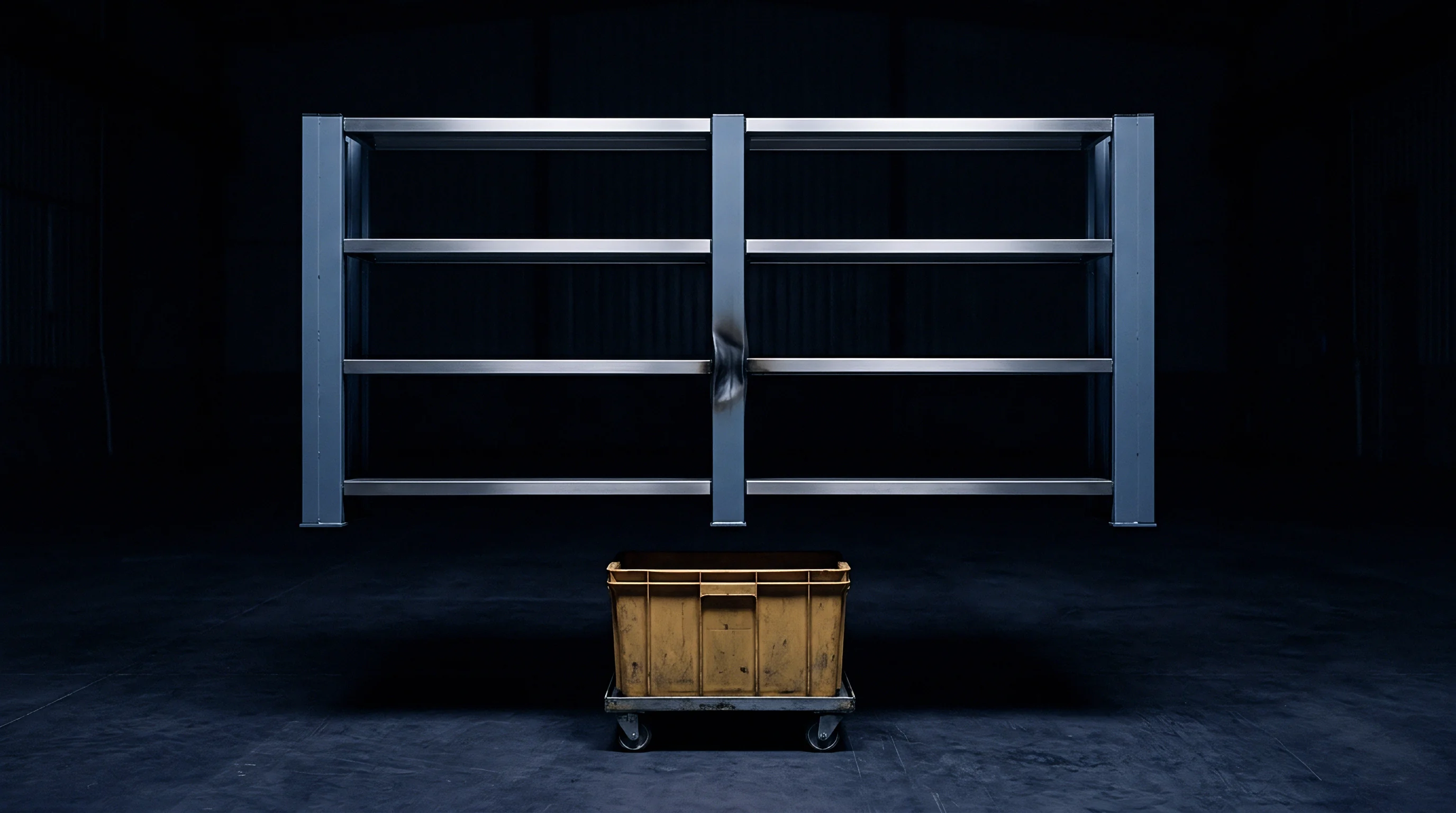

Peel

Stress Concentration at Free Boundaries
Bimaterial terminations concentrate normal and shear stresses within an edge zone roughly equal to layer thickness. Under extreme thermal gradients, the through-thickness heat transfer profile establishes a severe bending moment. This moment produces intense normal peel stresses along the outer peripheral boundary.
When brittle ceramic metallizations experience rapid cool-down from operating temperatures above 450 Kelvin, localized edge peel stresses frequently surpass 120 megapascals.
The mechanical field within this boundary zone cannot be resolved using simple beam theory. Finite element simulations and analytical boundary formulations show that normal stress exhibits a singular profile as the crack tip approaches the exterior free surface. The presence of tiny manufacturing voids, copper edge burrs, or solder flux residues within this high-stress margin provides immediate initiation sites for sub-surface delamination cracks.
Once started, these edge cracks advance inward toward active component areas.
| Interface Material Pair | Expansion Differential (ppm/K) | Peak Interface Shear (MPa) | Peak Edge Peel (MPa) | Interfacial Toughness (J/m²) |
|---|---|---|---|---|
| Copper / Silicon Nitride | 13.8 | 215 | 142 | 42 |
| Copper / Aluminum Oxide | 10.2 | 178 | 118 | 28 |
| Aluminum / Silicon Carbide | 19.5 | 285 | 195 | 35 |
| Silver Sinter / Silicon Carbide | 15.4 | 164 | 105 | 18 |
These localized peak stresses trigger catastrophic structural peeling when thermal transient frequencies match thermal diffusion response times. Rapid switching events in dense power converters produce cyclic thermal wavefronts that repeatedly load the free edges. Plastic deformation accumulates in metallic layers during peak heat periods, preventing complete stress relaxation during cooling.
Residual tensile stress accumulates with each thermal cycle, driving microcrack extension along the interfacial boundary.

Mixed-Mode Fracture Mechanics of Crack Extension
Crack tip behavior along bimaterial interfaces involves coupled opening and shearing displacement modes. The mode-mixity phase angle determines whether an existing defect advances cleanly along the material boundary or kinks into adjacent bulk phases. Extreme temperature gradients continuously shift this phase angle throughout dynamic thermal transients.
A crack initiating under pure shear can rapidly shift toward mode I tensile opening as the thermal wavefront penetrates into adjacent substrate layers.
The critical energy release rate varies strongly as a function of the mode-mixity phase angle. Interfacial toughness reaches a minimum under pure tensile opening, while frictional contact along crack surfaces increases apparent toughness under dominant shear. When steep thermal gradients induce out-of-plane warping, tensile peel stresses dominate, driving interfacial fracture energy to its lowest resistance threshold.
Microcracks spread rapidly along the interface during this vulnerable transient window.
The following sequence traces the physical progression of interfacial peel failure under extreme thermal gradients:
- Transient thermal wave penetration establishes steep through-thickness strain gradients before base temperatures shift.
- Localized plastic deformation accumulates within ductile metallization layers adjacent to the rigid substrate.
- Microcrack initiation occurs at boundary stress concentrations, voids, or microstructural inclusions along the interface plane.
- Phase-angle shifting swings local crack tip loading toward mode I tensile opening as the heat wave diffuses into lower layers.
- Unstable crack advance proceeds along the bonded interface until thermal equilibrium relieves the gradient driving force.
Failure to account for edge peeling results in rapid component cracking during early thermal shock testing.

Quench

Transient Cooling Cycles and Thermal Shock Severity
Rapid liquid cooling or cryogenic spray quenching imposes the most destructive stress gradients on bonded structural assemblies. While heating generates surface compression, severe quench events produce surface tensile stress fields that immediately pull at interfacial joints. Liquid nitrogen exposure, water immersion quenching, and rapid cold-plate activations create instantaneous surface temperature drops exceeding 1000 Kelvin per second.
Heat leaves the exterior layer long before core layers contract, setting up powerful through-thickness tensile stress distributions.
Under these transient quench conditions, the outer surface tries to contract against the warm, unyielding core material. This physical mismatch generates high in-plane tension at the outer layer and severe interfacial shear directly beneath it. The magnitude of this shear depends on the Biot number of the system, which compares internal conductive resistance to external convective heat transfer.
High Biot numbers signify steep temperature differentials across thin cross-sections, maximizing interfacial mechanical stress.
ASTM C1499 test protocols require rigorous calibration of thermal boundary conditions to prevent spurious edge failures during transient thermal evaluations.
Material selections must balance thermal conductivity and thermal expansion coefficients to withstand repeated quench events. Silicon nitride offers superior mechanical strength and fracture toughness compared to alumina, but still faces severe interfacial shear when bonded to thick copper layers. Rapid cooling of direct bonded copper assemblies from soldering temperatures produces immediate delamination along perimeter zones if cooling rates exceed twenty Kelvin per minute.
Managing these thermal descent rates remains essential for maintaining bond integrity.

Can Cyclic Thermal Shock Profiles Cause Progressive Delamination?
Repeated transient thermal cycles cause progressive interfacial degradation through cumulative ratcheting. Each quench cycle introduces plastic strains into ductile interlayers such as solder joints or metallic interposers. When thermal cycles repeat hundreds of times, unrecovered plastic strains accumulate along the interface boundary.
This ratcheting mechanism generates voids and micro-delaminations that gradually merge into extensive macroscopic debonding zones.
| Substrate Base Chemistry | Initial Delamination Area (%) | Final Delamination Area (%) | Thermal Resistance Increase (%) | Acoustic Void Density (cm⁻²) |
|---|---|---|---|---|
| Standard Al₂O₃ Substrate | 1.2 | 24.8 | 68 | 46 |
| Zirconia-Toughened Alumina | 0.8 | 12.4 | 31 | 19 |
| Silicon Nitride High-Rel | 0.3 | 2.1 | 6 | 3 |
| Aluminum Nitride DBC | 1.5 | 38.2 | 112 | 82 |
High thermal resistance across delaminated interfaces creates destructive operational feedback loops. As microcracks spread, local thermal resistance jumps, reducing the rate of heat removal from active device areas. This thermal dam elevates internal operating temperatures, sharpening local thermal gradients along the intact boundary perimeter.
Thermal stresses intensify around the delamination front, accelerating crack advance across the remaining bonded area.
Ultrasonic inspection maps reveal that crack advance during cyclic quenching proceeds in discrete jumps corresponding to individual peak thermal gradients. High cooling rates trigger burst-like crack propagation events, whereas slow thermal transitions produce stable, sub-critical crack growth. The presence of residual assembly stresses from high-temperature braze cooling amplifies these cyclic shock damages, causing premature delamination during early operating lifecycles.
Suppliers frequently suggest that minor edge debonding observed after thermal shock testing represents an isolated cosmetic anomaly.

Anchor

Engineered Interlayers and Functionally Graded Boundaries
Mitigating stress gradient coupling requires structural solutions that smooth the sharp mechanical discontinuity across the bonding plane. Traditional direct-bonded joints present a step change in elastic modulus and thermal expansion coefficient across an atomic boundary. Introducing engineered interlayers or functionally graded transitions distributes the thermal mismatch over a wider structural volume, reducing peak interfacial shear stresses.
Deposition of compliant metallic interlayers, such as electroplated nickel, sputtered titanium-platinum-gold, or thin silver sinter networks, provides local plastic compliance that absorbs transient thermal displacement mismatches. These buffer layers deform under shear, lowering the peak peeling stresses transmitted to brittle ceramic substrates. The thickness of this compliant zone must be engineered carefully: insufficient thickness fails to alleviate stress concentrations, while excessive thickness increases total thermal resistance across the joint.
Compliance interlayers absorb displacement mismatches through localized micro-yield behavior without transferring critical peeling moments to brittle ceramic substrates.
Functionally graded materials provide another robust design approach by progressively shifting composition from metal to ceramic over several micrometers. By eliminating discrete mechanical interfaces, graded boundaries remove the planar singularity that drives mixed-mode interfacial delamination. Modern additive manufacturing, spark plasma sintering, and plasma spray methods allow precise continuous grading of material chemistry, matching thermal and mechanical properties across extreme operational environments.
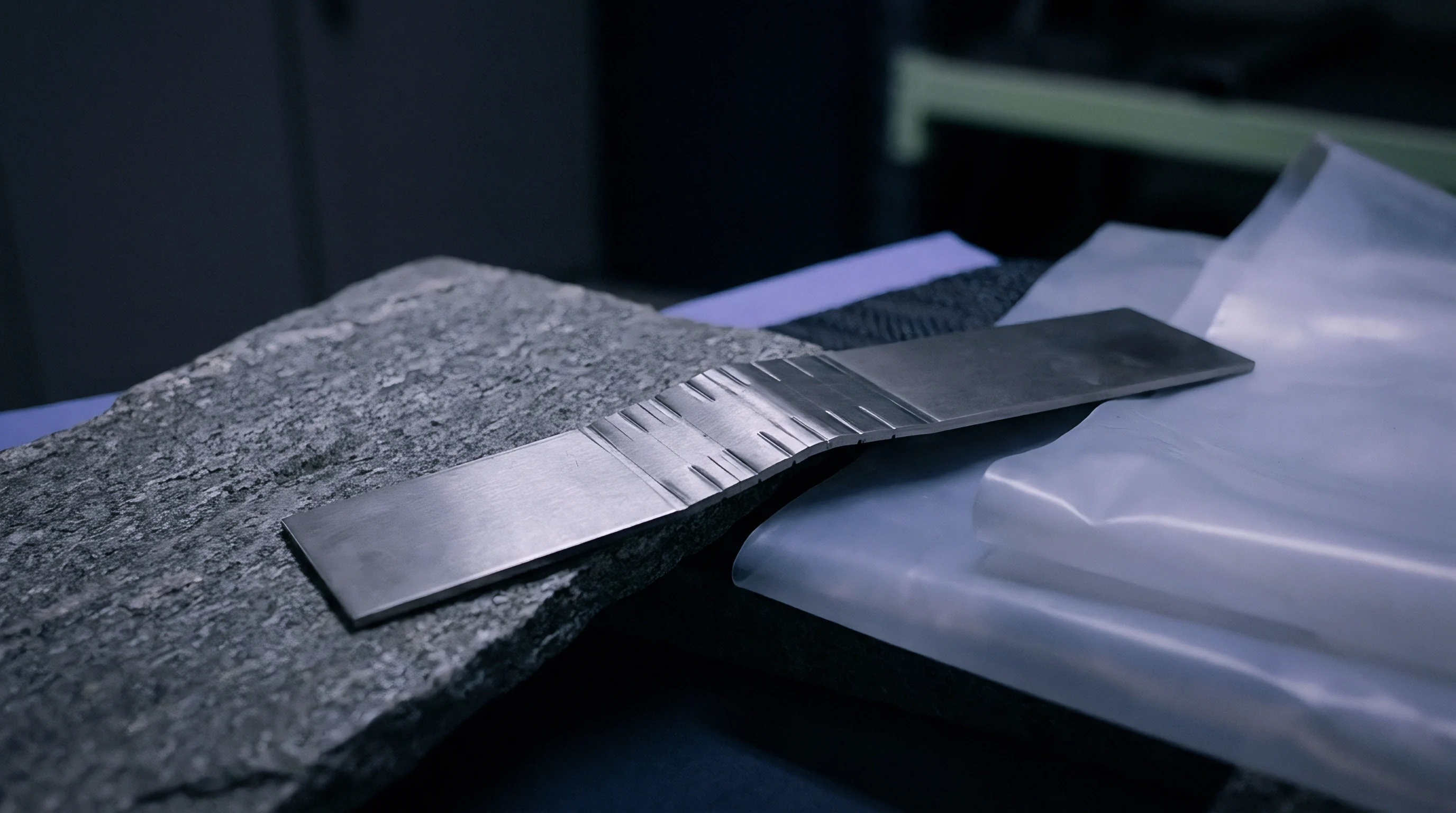
Surface Micromorphology and Mechanical Interlocking
Micro-texturing the substrate surface before bonding significantly improves resistance to interfacial delamination under thermal shock. Chemical micro-etching, laser ablation, and wet chemical texturing generate micro-scale roughness profiles that provide mechanical interlocking sites. When a metallic layer is bonded to an engineered micro-textured surface, propagating cracks encounter local geometric barriers that force continuous deflection out of the weak interfacial plane.
These geometric deviations force the crack tip to kink repeatedly into tougher bulk materials, substantially increasing apparent interfacial fracture toughness. Crack kinking dissipates mechanical strain energy and reduces the local crack driving force. Chemical anchor profiles such as re-entrant cavities or micro-undercuts provide mechanical keying that resists normal mode I tensile opening even under severe out-of-plane edge peel stresses.
Key technical parameters governing mechanical anchor performance include:
- Arithmetic mean roughness between 1.5 and 3.5 micrometers ensures optimal braze or sinter paste penetration without creating unbonded micro-cavities.
- Re-entrant cavity density exceeding 200 sites per square millimeter establishes mechanical interlocking that resists normal tensile peel stresses.
- Chemical deoxidation cleanliness maintains surface oxide thickness below five nanometers, preventing premature interfacial cohesive fractures.
- Interlayer modulus compliance below 80 gigapascals accommodates transient shear displacements through localized plastic flow mechanisms.
Excessive surface roughness without proper vacuum degassing creates unbonded gas pockets that act as pre-existing edge cracks during subsequent thermal quench cycles.

Gauge

In Situ Diagnostics and Acoustic Wave Spectroscopy
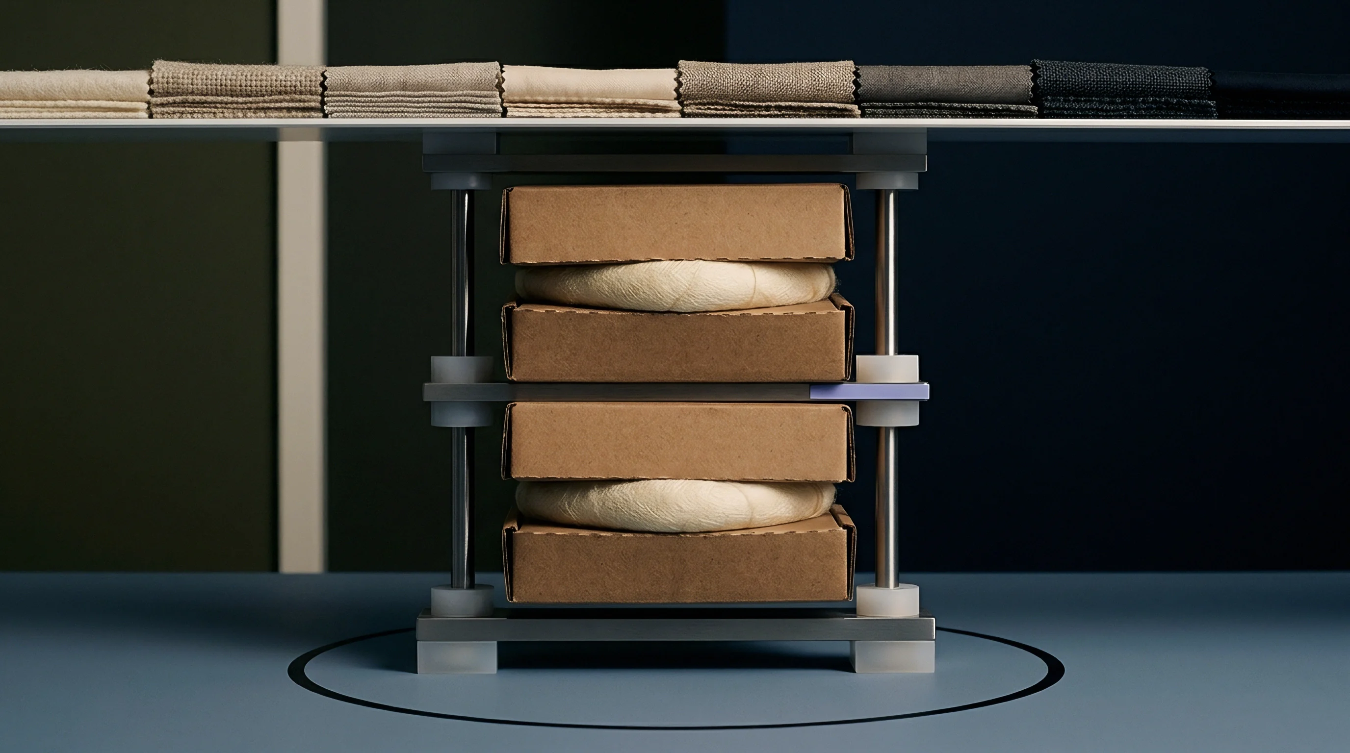
Quantifying interfacial delamination mechanics under dynamic thermal gradients requires high-resolution diagnostic instruments. Static post-mortem cross-sectioning fails to capture transient crack movements that open during peak temperature extremes and snap shut during thermal equilibrium. Advanced nondestructive evaluation techniques monitor crack initiation and crack propagation paths during live thermal shock exposure.
High-frequency scanning acoustic microscopy provides sensitive detection of sub-surface delamination interfaces. Utilizing focused transducers between 50 and 230 megahertz, acoustic microscopy detects air gaps and disbond layers thinner than ten nanometers through acoustic impedance mismatch reflections. Real-time acoustic emission sensors mounted on the specimen fixtures record high-frequency acoustic waves generated by sudden micro-cleavage events, pinpointing the precise second and temperature threshold of initial crack advance.
| Diagnostic Technique | Spatial Resolution (µm) | Minimum Disbond Thickness | In Situ Thermal Capability | Inspection Depth Range |
|---|---|---|---|---|
| Scanning Acoustic Microscopy | 5 to 15 | 5 to 10 nm | Limited to Room Temp | Up to 5 mm |
| X-Ray Micro-Computed Tomography | 1 to 3 | 500 nm | High Temp Chambers | Full Assembly Penetration |
| Pulsed Phase Thermography | 100 to 200 | 1 to 2 µm | Dynamic In Situ Real Time | Up to 1.5 mm |
| Laser Ultrasonic Inspection | 20 to 50 | 50 nm | High Temp Compatible | Up to 10 mm |
Pulsed thermography mapping measures the surface temperature response following a high-energy optical flash. As heat diffuses through the assembly, interfacial delaminations act as thermal barriers that trap heat at the surface, creating distinct hot-spot footprints on infrared cameras. Correlating transient thermographic profiles with finite element thermal models allows precise quantification of local disbond dimensions and interfacial thermal contact resistance.

Defect Detection Thresholds and Inspection Verification
Verifying interfacial integrity in production environments requires establishing explicit defect acceptance thresholds tied to operating thermal gradient severities. Standard manufacturing quality checks relying solely on electrical continuity or bulk thermal resistance tests miss perimeter edge microcracks below 50 micrometers in length. These undetected microcracks provide ready propagation paths during dynamic operating cycles, eventually causing field failures.
Acoustic inspection criteria must define the maximum permissible unbonded area and clear keep-out zones along critical high-stress perimeters. IPC-A-610 and MIL-STD-883 standards establish general baseline acceptance criteria, but high-gradient applications require tighter tolerances. Edge delaminations exceeding 0.5 millimeters in inward depth cannot be accepted in severe thermal environments, as calculated edge peel stresses concentrate directly along the newly established crack tip.
A rigorous verification routine combines baseline scanning acoustic microscopy, a twenty-cycle liquid-to-liquid thermal shock exposure test, and secondary acoustic verification. Any growth in disbond area exceeding two percent of total joint surface area indicates inadequate bond toughness or excessive residual assembly stresses. Such parts must be isolated before committing downstream assembly resources.
Purchase specifications that omit non-destructive scanning acoustic microscopy parameters permit parts with critical sub-surface edge microcracks to enter final production.

Margin

Fracture Mechanics Bounds and Design Tolerances
Preventing interfacial delamination under extreme thermal gradients requires setting conservative design margins grounded in fracture mechanics. Engineers must balance thermomechanical properties across all substrate, metallization, and die-attach layers. When peak energy release rates remain strictly below 40 percent of the critical interfacial fracture toughness under worst-case thermal gradients, assemblies demonstrate high resistance to delamination.
Finite element calculations must explicitly incorporate temperature-dependent thermal expansion and elastic modulus properties. In ceramic-metal direct-bonded structures, the yield strength of the metallic layer drops rapidly at elevated temperatures, shifting interfacial stresses into plastic deformation modes. Conversely, during cold-start or rapid quench conditions, metal yield strength climbs, transmitting higher elastic shear and peel stresses directly into the brittle interface.
Safety margins must be validated across the complete temperature envelope.
| Material Designation | Elastic Modulus (GPa) | Thermal Conductivity (W/m·K) | CTE at -40°C (ppm/K) | CTE at 200°C (ppm/K) |
|---|---|---|---|---|
| Direct Bonded Copper | 115 to 130 | 385 to 395 | 15.2 | 17.8 |
| Silicon Nitride (Si₃N₄) | 300 to 320 | 80 to 90 | 2.4 | 3.2 |
| Aluminum Nitride (AlN) | 310 to 330 | 170 to 180 | 3.8 | 4.7 |
| Direct Bonded Aluminum | 65 to 70 | 210 to 225 | 21.5 | 24.6 |
Calculations show that rounding metallization edges and introducing perimeter dimples or relief trenches reduces localized stress concentration factors by up to 45 percent. Etching a step-back border along copper traces redistributes edge shear away from the outer ceramic perimeter, reducing the driving force below critical disbond limits. These minor geometric modifications prevent costly material substitutions while maintaining assembly reliability under steep thermal gradients.

Does Solder Voiding Shift the Delamination Threshold?
Interfacial voiding within solder joints and sintering layers alters the local stress gradient field. Rather than acting as benign empty pockets, large voids concentrate mechanical peel and shear stresses along their perimeters. Under extreme thermal fluxes, voids disrupt heat flow paths, creating hot spots with severe localized thermal gradients across adjacent bonded layers.
A void diameter exceeding twenty percent of total joint thickness increases local energy release rates by more than two times under transient thermal loading. Microcracks initiate at these high-stress void perimeters, spreading radially outward until they merge with adjacent voids or reach substrate free edges. Strict void inspection criteria must limit individual void areas to less than two percent of total pad area, with cumulative voiding kept below five percent in high-gradient power electronic modules.
The following design criteria govern structural margins under extreme thermal gradient regimes:
- Maximum transient energy release rate stays below 40 percent of measured mixed-mode interfacial fracture toughness.
- Perimeter edge step-back provides at least 0.5 millimeters of exposed substrate margin along active metallization borders.
- Maximum single-void diameter remains under fifteen percent of solder layer thickness across all thermal pads.
- Substrate corner chamfer radius exceeds 0.2 millimeters to eliminate acute geometric stress singularities.
Section 8.2 of the master supply agreement establishes that any batch showing interfacial delamination growth beyond two percent of the active pad area under forty thermal shock cycles triggers an immediate stop-shipment order and a full manufacturing audit.