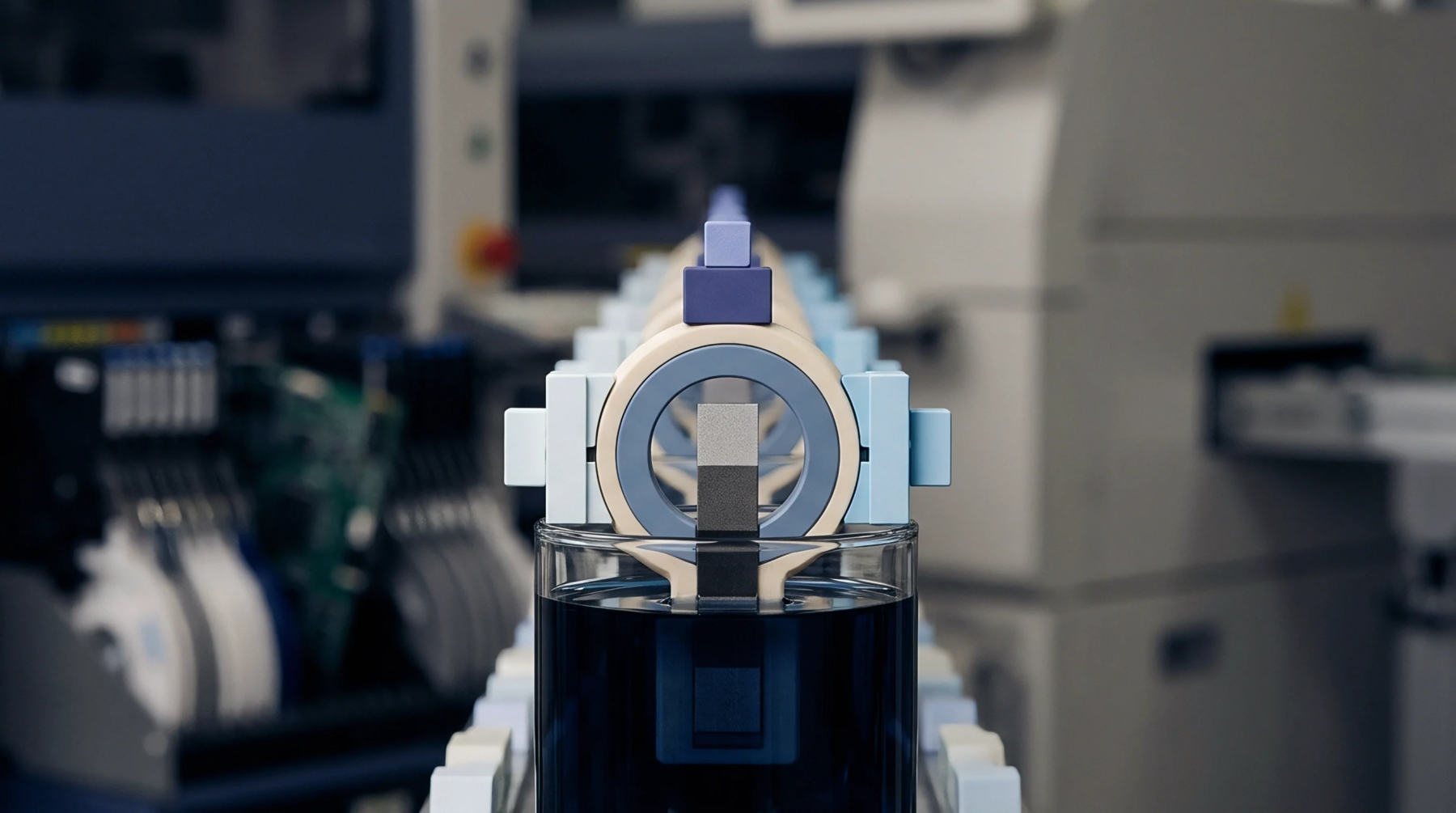
Stress Coupled Vacancy Migration Dynamics in Microelectronic Interconnect Substrates
Stress-coupled vacancy migration in substrate vias is controlled by managing copper grain texture, barrier adhesion energy, and post-plating anneal thermal budgets.
Self-forming barrier layer technologies in advanced semiconductor interconnect fabrication use specialized alloy mixtures to prevent metal diffusion into the dielectric material without requiring a separate deposition step. In the creation of sub-microscopic electrical connections, a copper-manganese seed is deposited directly onto the trench walls before the main copper electroplating process begins. This alloy layer contains a small percentage of manganese which reacts with the surrounding dielectric during a subsequent annealing step to form a super-thin manganese silicate barrier.
This chemical reaction creates a highly uniform and continuous barrier that prevents copper migration, which is essential for maintaining the insulation of the surrounding silicon dioxide. The use of this technology is limited to specific dielectric materials that contain silicon and oxygen, as the self-forming mechanism relies on the chemical reaction between these elements and the manganese atoms.
Diffusion-driven chemical reactions during the thermal annealing phase generate a protective oxide layer at the interface between the metal line and the insulating dielectric. When a copper-manganese seed is heated to temperatures between three hundred and four hundred degrees Celsius, the manganese atoms migrate toward the dielectric interface because of their high affinity for oxygen. Once they reach the dielectric, they react with the silicon dioxide to form a continuous layer of manganese silicate that is only a few nanometers thick.
This self-forming barrier is much thinner and more uniform than the tantalum barriers deposited by conventional sputtering methods, which is critical for very narrow trenches where every nanometer of conductor volume is valuable. The remaining copper in the seed layer becomes highly purified as the manganese leaves, which maximizes the electrical conductivity of the finished interconnect.
Grain boundary reinforcement achieved through the segregation of minor alloying elements improves the mechanical stability of the conductor under high current densities. During the operation of the integrated circuit, some of the manganese from the copper-manganese seed remains at the grain boundaries of the copper line, where it acts as a pinning agent that restricts the movement of copper atoms. This structural reinforcement significantly reduces the rate of electromigration, which is the primary cause of open-circuit failures in advanced microprocessors.
The presence of manganese at the interfaces also strengthens the adhesion between the copper and the dielectric, preventing the formation of voids along the top surface of the metal line. These dual benefits make the alloy seed technology highly attractive for manufacturing high-performance computing chips that operate under high electrical and thermal loads.
Equipment configuration and process sequence optimization are required to integrate alloy seed deposition into standard semiconductor manufacturing lines. To successfully apply a copper-manganese seed, the deposition chamber must maintain an extremely low base pressure to prevent the premature oxidation of the manganese before it reaches the wafer surface. The composition of the alloy target must be controlled to ensure that the concentration of manganese in the deposited film remains within the specified range, typically between one and five percent.
If the manganese concentration is too high, the residual manganese in the copper lines will increase the electrical resistance of the interconnects, defeating the purpose of the technology. Regular monitoring of the metal composition using x-ray photoelectron spectroscopy ensures that the alloy composition remains stable across successive production runs.
Stress-coupled vacancy migration in substrate vias is controlled by managing copper grain texture, barrier adhesion energy, and post-plating anneal thermal budgets.
Expertise is a utility, not a secret. sentiention™ publishes its working knowledge as open reference: intelligence layer covering the materials it sources, the markets it enters, and the reference that serves both.