Step Height Calibration Standards for Non Contact Metrology
Certified step standards align non-contact metrology tools across supply chains, eliminating phase anomalies, tool drift, and expensive production scrap.


Trace
Calibration artifacts for non-contact optical profilometry and white light interferometry sit inside cleanroom storage boxes across semiconductor and advanced packaging facilities, holding traceable step heights intended to govern micron-scale vertical metrology. The physical height certified on an inspection document from the National Institute of Metrology in Beijing or the National Institute of Standards and Technology in Gaithersburg does not transfer automatically to an optical sensor. Non-contact instruments rely on light reflection, spatial coherence, phase shifts, and electronic algorithms to construct a step height profile.
Optical artifacts like diffraction batwings, material-dependent phase discontinuities, and localized curvature distort the measurement. The certified reference height defines the baseline geometry, while optical physics dictates the actual reading generated by an imaging sensor.
Production facilities that fabricate silicon wafers, microfluidic channels, or display backplanes often discover height discrepancies between contact stylus profilers and coherence scanning interferometers. stylus tips push through surface contamination and track mechanical boundaries directly. Optical beams interact with complex refractive indices, edge gradients, and transparent passivation films, shifting the apparent boundary position. When two metrology stations disagree across an assembly pipeline, the mechanical dispute turns into a dispute over shipping schedules, lot acceptance, and rework responsibility.
Optical edge diffraction introduces height measurement artifacts that mechanical stylus needles bypass completely.
Traceability chains for step height artifacts depend on explicit reference geometries. A calibrated target requires documentation that links its measured value through unbroken comparison stages directly to the standard meter definition realized via stabilized helium-neon lasers at 632.8 nanometers wavelength. Without direct traceability documentation, an artifact functions only as a relative repeatability coupon.
The standard reference geometry comprises an etched groove, a raised mesa, or a sequence of calibrated finger structures fabricated into silicon, fused silica, or quartz substrates. Each structure provides defined plateaus separated by vertical transitions ranging from 10 nanometers to over 100 micrometers. Optical systems capture these features under specific numerical apertures and illumination wavelengths, meaning that an artifact calibrated under one optical geometry can generate systematic offsets when placed on an alternative tool.
Factory engineers handling automated inspection systems in Suzhou or Shenzhen often encounter step height disputes during process transfers from overseas development lines. Equipment vendors cite internal factory calibration logs that show sub-nanometer instrument noise floors, while incoming silicon exhibits step discrepancies exceeding fifteen percent of nominal tolerances. Resolving these measurement disagreements requires matching the calibration artifact’s physical layout and optical properties to the specific non-contact measuring system in the production line.


Beam
White light interferometry, confocal microscopy, and focus variation systems each collect vertical position information through distinct optical paths. Every approach reacts differently to the sharp step transition on a calibration artifact. The physical standard presents an abrupt edge discontinuity, which truncates the reflected wavefront and creates spatial frequency losses across the objective lens collection cone.
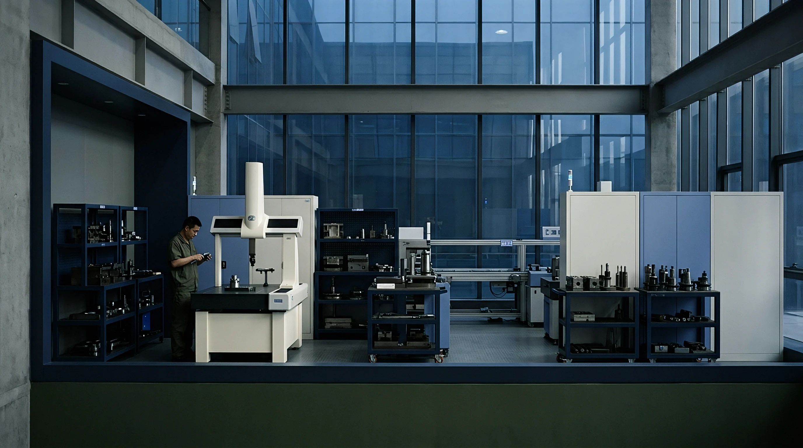
Optical Phase Shift at Material Boundaries
A step height artifact etched into bare silicon and coated partially with chrome introduces phase anomalies during interferometric measurement. The complex refractive index of the materials governs light reflection behavior. Silicon presents a complex index of approximately 3.88 + 0.02i at 633 nanometers, whereas vacuum-deposited chromium exhibits an index around 3.15 + 3.32i.
This difference alters the phase change upon reflection between the top plateau and the trench base.
Interferometers convert this phase difference directly into an apparent physical height shift. When an optical profiler measures a step standard constructed from mixed materials, the reported step height deviates from the physical geometric height by several nanometers. Single-material artifacts, produced by etching directly into silicon or quartz followed by uniform gold or platinum sputtering, eliminate differential reflection phase errors.
Monolithic surfaces guarantee identical optical phase responses across both upper and lower boundaries.

Diffraction Spikes and Plateau Extraction Methods
Diffraction at the edge of a step artifact produces spurious signals, commonly called batwing anomalies, within coherence scanning interferograms. As the optical scanning head passes the vertical boundary, light scattered from the top plateau interferes with light emerging from the trench bottom. The instrument software reconstructs an artificial peak or trough at the edge transition.
Filtered algorithms mitigate these diffraction spikes by applying standardized evaluation windows across the upper and lower traces. ISO 5436-1 defines the formal mathematical construction for step height determination, excluding the transition zones to avoid diffraction errors. The standard mandates leaving a central portion of each plateau for statistical evaluation, rejecting the inner regions adjacent to the edge step.
| Metrology Technology | Measurement Principle | Step Height Limit | Primary Edge Artifact |
|---|---|---|---|
| Coherence Scanning Interferometry | Broadband white light fringe visibility localization | 0.1 nm to 5 mm | Batwing diffraction peaks at abrupt edges |
| Phase Shifting Interferometry | Monochromatic phase step reconstruction | 0.1 nm to 150 nm | Phase ambiguity wraps past quarter-wavelength |
| Laser Scanning Confocal | Pinhole spatial filtering of focal planes | 50 nm to 20 mm | Signal broadening at non-perpendicular sidewalls |
| Focus Variation Microscopy | Local contrast evaluation across depth of field | 300 nm to 50 mm | Edge rounding across specular mirror surfaces |
Focus variation systems struggle with mirror-smooth reference artifacts. Because focus variation requires scattered surface texture to calculate sharp local contrast, specular gold-coated calibration steps produce zero signal across horizontal flats. An artifact engineered for white light interferometry fails to function on a focus variation instrument without added microscopic roughness.
Step standards must match the optical detection method of the target instrument.
Objective numerical aperture governs lateral resolution and diffraction behavior. A 50x objective with a 0.80 numerical aperture collects higher spatial frequencies, capturing edge steps with minimal batwing width. A 5x objective with a 0.15 numerical aperture spreads the edge diffraction zone across multiple micrometers, corrupting smaller calibration plateaus.
The calibration certificate remains valid only when the field of view isolates the flat reference plateaus away from the diffraction boundary.

Etch
Fabricating certified step height standards requires advanced semiconductor microfabrication techniques to maintain nanometer-scale vertical accuracy and low surface roughness. Commercial suppliers employ anisotropic reactive ion etching, wet chemical etching, or thermal oxide growth on monocrystalline silicon wafers. The production methodology determines sidewall angles, base planarity, and long-term mechanical stability.
Thermal oxidation of silicon substrates provides stable steps below 100 nanometers. Technicians grow silicon dioxide layers under controlled oxygen atmospheres at temperatures above 1000 degrees Celsius, followed by photolithographic patterning and buffered oxide etching. The etched oxide boundary presents steps down to single-nanometer dimensions with surface roughness below 0.2 nanometers Ra. The oxide step exhibits durability, resisting common ultrasonic solvent cleaning regimens.
Deep vertical structures above 1 micrometer demand reactive ion etching into bulk silicon substrates. Etch uniformity across an eight-inch substrate varies with plasma distribution and gas dynamics. Microloading effects cause narrower trenches to etch slower than wider reference areas, leading to depth variations across adjacent features.
Certified step artifacts isolate calibration features from microloading zones by spacing pitch structures away from single step plateaus.
- Silicon Dioxide Steps provide exceptional baseline planarity for thin standards under two hundred nanometers, utilizing thermal growth regimes to maintain sub-nanometer thickness tolerances across broad wafer territories.
- Silicon Reactive Ion Etching yields durable monolithic targets extending past fifty micrometers depth, though sidewall scalloping and localized micro-trenching require rigorous atomic force microscopy inspection during factory qualification.
- Quartz Mesa Features offer thermal expansion stability matching optical stage components, minimizing temperature-induced drift within high-throughput cleanroom operating environments.
- Polymer Precision Films serve as cost-effective vertical references for coarse tactile and focus variation metrology, but degrade rapidly under concentrated ultraviolet laser illumination and strong solvent cleaning agents.
Sidewall angles present distinct challenges for non-contact metrology tools. Chemical wet etching on (100) silicon produces characteristic 54.7-degree crystal plane slopes along (111) boundaries. Vertical reactive ion etching produces near-90-degree cliffs.
Optical instruments cannot collect light reflected from perpendicular sidewalls, causing missing data points or extreme noise spikes at vertical boundaries. Calibration algorithms interpolate across these blind zones using data extracted from the upper and lower horizontal planes.
Thin film coatings deposited over step structures protect against environmental corrosion and balance optical reflectivity. Chromium adhesion layers topped with gold coatings provide broad optical reflectivity across visible and infrared spectrums. Sputtering processes introduce residual internal stress, which causes thin reference steps to bend or bow across millimeter spans.
Substrates must undergo thermal annealing cycles to relieve internal stress prior to metrological certification.
A supplier quoting calibration standards might claim certified accuracy across every feature on a multi-pitch reticle. Yet uninspected process drift during plasma etching leaves peripheral features outside certified tolerances. A buyer must verify that the calibration certificate applies to the specific, numbered feature within the reticle field rather than a broad batch witness sample.

Drift
Physical artifacts degrade through environmental exposure, organic film accumulation, mechanical cleaning, and thermal changes within factory inspection cells. A silicon step standard left inside a cleanroom without sealed container protection collects airborne molecular contaminants. Organic films deposit at rates between 0.2 and 0.8 nanometers per month, shifting the absolute height recorded by optical instruments.

Surface Contamination and Cleaning Risks
Hydrocarbon layers alter both physical dimensions and surface reflectivity. Phase shifting interferometers are sensitive to ultra-thin transparent dielectric films, where an organic contamination layer causes unexpected phase changes upon reflection. The instrument registers this contamination layer as a height error during certification routines.
Aggressive manual cleaning with contact swabs scratches soft reflective coatings like gold or aluminum. Even light contact creates micrometer-wide scratches that disrupt the flat plateau areas required by ISO 5436-1 calculations. Ultrasonic bath cleaning risks delaminating sputtered metal films from underlying silicon dioxide layers if the initial chromium adhesion layer was deposited improperly.
Solvent vapor cleaning protocols preserve fragile metal layers that mechanical swabbing strips away.
Liquid solvent cleaning requires spectrophotometric grade solvents to avoid leaving non-volatile residues. Standard cleaning uses an ultrasonic rinse in high-purity isopropyl alcohol, followed by a dry nitrogen blow-off under static-neutralizing bars. When heavy organic films accumulate, ultraviolet ozone cleaning strips hydrocarbon compounds without contacting the fragile optical surface.
Standards showing deep scratches across plateau areas must be retired, as damaged reference zones yield invalid calibration values.

Thermal Expansion and Environmental Control
Thermal stability inside the metrology enclosure directly affects measurement reliability. The thermal expansion coefficient of monocrystalline silicon sits at 2.6 parts per million per degree Celsius, while fused silica sits at approximately 0.5 parts per million. A four-degree Celsius temperature shift in a production area alters a 100-micrometer step by fractions of a nanometer, which is small compared to typical manufacturing tolerances.
However, thermal fluctuations expand the metrology tool’s structural frame and internal optical mountings, introducing drift that corrupts precision measurements.
| Mechanism | Physical Manifestation | Impact on Measurement | Corrective Action |
|---|---|---|---|
| Hydrocarbon Adsorption | Organic boundary film accumulation | Phase errors from 0.5 nm to 3 nm | Controlled ultraviolet ozone cleaning |
| Abrasive Cleaning | Scratches and material removal | Plateau roughness exceeding Ra limits | Retirement and artifact replacement |
| Substrate Bowing | Biaxial mechanical stress release | Loss of planarity across baseline | Recalibration using wide-area tilt compensation |
| Oxide Layer Growth | Native oxide formation on bare silicon | Drift of 0.1 nm per year | Recalibration against laser standards |
Managing artifact degradation requires setting strict recalibration intervals. Metrology facilities establish re-certification cycles between 12 and 24 months, sending artifacts back to accredited laboratories for verification against primary laser displacement standards. Calibration histories that show ongoing baseline changes highlight structural damage or surface contamination, invalidating past inspection data.
The metrology technician records ambient temperature, relative humidity, and barometric pressure at the start of each daily instrument check. Optical interferometers operating in uncontrolled factory air experience optical path length variations caused by air density fluctuations. When ambient conditions drift beyond instrument operating specifications, internal baseline readings lose sub-nanometer repeatability.
Ledger
Step height standards represent capital investments and operational control points within cross-border supply chains. Standard pricing tracks certified manufacturing difficulty, ranging from several hundred dollars for coarse, uncertified diagnostic chips to tens of thousands of dollars for multi-pitch, NIST-traceable quartz artifacts. Purchasing decisions balance product tolerance requirements against the financial exposure of scrap parts and assembly disputes.

Calculating Metrological Risk across Borders
Consider an assembly line producing advanced optical packaging modules with an operational budget based on the following manufacturing parameters:
The manufacturing facility targets 50,000 components per month at an assembly cost of 48 dollars per finished unit. The critical specification requires a wire-bond pad step height of 12.50 micrometers with an allowable process tolerance of plus or minus 0.50 micrometers. The facility operates an uncalibrated optical profiler that drifts by 0.12 micrometers over a three-week run due to thermal cycling and unverified software baseline parameters.
This 0.12-micrometer measurement offset consumes 24 percent of the total allowable tolerance budget. The metrology tool begins rejecting good components near the tolerance edge while passing out-of-spec modules to downstream customers. If the false rejection rate reaches 3.2 percent across the monthly production volume, the factory scraps 1,600 acceptable parts each month.
The direct financial loss totals 76,800 dollars every month in discarded assemblies.
Investing in two certified step height reference standards at 6,500 dollars each, supported by a 2,200-dollar annual calibration retainer, stabilizes the measurement baseline. Daily artifact checks catch instrument drift within 15 minutes of occurrence. The calibration cost pays for itself within the first week of prevented product scrap.
Disputes between overseas product design teams and domestic fabrication facilities often trace back to unaligned calibration standards. An overseas brand team uses an automated coherence scanning interferometer calibrated against a quartz step standard, while the assembly contractor in Dongguan verifies parts using an uncertified laser confocal microscope. Both parties run their tools within manufacturer parameters, yet their inspection records disagree by 200 nanometers.
This measurement offset stalls engineering approvals, delays production milestones, and incurs air-freight surcharges while teams investigate the root cause.
Procurement agreements must include explicit metrology clauses that specify artifact model numbers, calibration frequency, and authorized calibration laboratories. When purchase orders omit step height calibration protocols, the buyer absorbs the cost of dimensional disagreements during factory acceptance tests.

Protocol
Translating calibration certificates into dependable factory operations requires structured measurement procedures. Quality engineers implement standardized verification steps to isolate tool optical errors from operator handling mistakes. An established measurement protocol prevents production lines from drifting outside defined quality control limits.
- The cleanroom technician retrieves the certified calibration artifact from its desiccated nitrogen storage cabinet, verifying that the protective carrier remains free of physical seal damage.
- The technician inspects the artifact surface under a low-power optical microscope using darkfield illumination to confirm the absence of dust particles, organic streaks, or mechanical scratches across the certified evaluation fields.
- The technician places the standard upon the vibration-isolated metrology stage, allowing fifteen minutes for thermal equilibrium between the sample holder, the silicon artifact, and the microscope objective lens.
- The operator aligns the step boundary perpendicular to the instrument camera axis, minimizing lateral tilt across the horizontal plateaus through automated tip-tilt stage adjustment routines.
- The operator configures the measurement software to execute five successive scans across the identical certified region, applying the standard ISO 5436-1 boundary masking filters to calculate the mean step height and standard deviation.
- The quality manager compares the recorded mean step height against the certified calibration value, initiating corrective instrument recalibration if the measurement delta exceeds three times the tool noise threshold.
Data processing algorithms determine the final reported step height. Modern optical profilers include proprietary edge-finding and plateau-fitting routines in their factory software. Quality teams must verify that instruments use standardized algorithms like ISO 5436-1 rather than unverified vendor-specific routines, as unstandardized filtering can mask underlying measurement drift.
Equipment suppliers frequently balance edge diffraction noise using aggressive smoothing filters that distort underlying physical step profiles.
Instrument operators must also track environmental conditions during routine tool qualifications. Metrology logs require documentation of ambient temperature, humidity levels, objective lens magnifications, and optical filtering settings alongside recorded calibration heights. Incomplete calibration logs prevent root-cause analysis when dimensional disputes emerge between shift teams or across distributed production facilities.
Cross-border production managers reduce measurement disagreements by maintaining a dedicated set of golden calibration artifacts. The engineering team retains one set at headquarters while providing an identical, traceable set to the manufacturing facility. Aligning calibration standards across both sites ensures that internal inspection logs match incoming quality audits at customer delivery docks.
A supplier quality lead often claims that internal software self-checks remove the need for daily physical artifact measurements. That explanation fails to account for dirty objective lenses, mechanical stage wear, and internal illumination drift. Daily artifact checks provide physical proof of instrument accuracy, protecting both the supplier and the customer from measurement disputes.